Why Choose HXD for Your 10-Layer PCB?
Manufacturing a 10-layer PCB is a highly complex process, far more challenging than making 2-layer or 4-layer boards.HXD has many years of experience and a mature manufacturing system in the 10-layer PCB field.
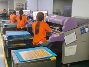
Lamination Equipment
HXD is equipped with advanced vacuum lamination systems to ensure tight bonding of multilayer structures under high temperature and high pressure.To prevent interlayer misalignment, we use a CCD + IR hybrid alignment system. keeping layer-to-layer tolerance at ≤25μm or even tighter.
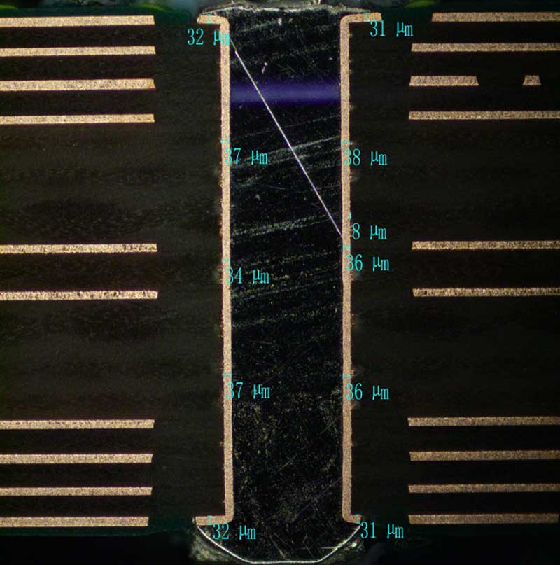
High-Precision Drilling Technology
Manufacturing 10-layer PCBs often requires drilling with high aspect ratios (up to 16:1).10-layer PCBs often require drilling with high aspect ratios (up to 16:1). HXD uses both Laser Drilling for microvias and CNC Mechanical Drilling for standard holes.Our capabilities include:
- Small Hole Diameters: Precision drilling for holes smaller than 0.15mm.
- Microvia Technology: Laser-drilled holes for high-density interconnects.
Laser Direct Imaging(LDI)
For high-precision circuits, HXD utilizes LDI technology. This ensures maximum accuracy for fine-line patterns, such as 2.5/2.5 mil trace and space.
HDI & Microvia Technology
We are experts in Blind Vias, Buried Vias, and Laser Microvias. These technologies are essential for 10-layer High-Density Interconnect (HDI) designs.By utilizing these advanced techniques, we help you achieve higher integration and smaller form factors within limited board space.
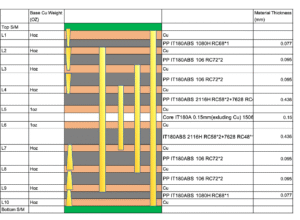
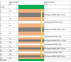
Specialty Materials & Hybrid Lamination
HXD has the expertise to process a wide range of high-performance substrates, including high-performance FR-4, Rogers, and Isola.
We also support hybrid lamination of high-frequency materials with standard materials, helping you balance performance and cost while meeting application needs.