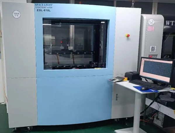
100% Electrical Testing
Every board is fully tested for open circuits, short circuits, and net continuity before shipment. We use flying probe or fixture-based testing depending on volume, ensuring zero electrical defects reach your assembly line.
Our PCB Manufacturing Capabilities cover PCB Fabrication services for double-sided PCB, multilayer PCB, HDI PCB, aluminum PCB, heavy copper PCB, Rogers PCB, and high-frequency PCB projects.
You can also use our PCB Material Selector and PCB Stackup Design tool to compare materials, plan layer structures, and prepare your design for prototype or production.
| Items | Standard PCB | Advanced PCB |
|---|---|---|
| Board Type | Rigid, Rigid-Flex,Flex,HDI,hybrid Laminating | / |
| Layers Count | 2–16 layers | 18–20 layers & HDI products |
| Finished Board Thickness | 16~128 mil (0.4mm – 3.2mm) | / |
| Max. Panel Size | 24 × 28.5″ (622mm × 723mm) | 24 × 40″ (622mm × 1000mm) |
| Laminate Materials | FR-4, Aluminum, Copper Base,PTFE,Ceramic, Polymide, Rogers, PTFE, ISOLA, Panasnic | / |
| Finished Board Thickness Tolerance | < 1.0mm ±0.10mm (±4mil) 1.0~1.6mm ±0.15mm (±6mil) | < 1.0mm ±0.075mm (±3mil) 1.0~1.6mm ±0.10mm (±4mil) |
| Min. Inner Thin Core Thickness | 3mil (0.075mm) | / |
| Min. Inner Line Width / Spacing | 2.5 / 3.5 mil (0.0635 / 0.089mm) | 2.5 / 2.5 mil (0.0635mm) |
| Min. Outer Line Width / Spacing | 3.5 / 3.5 mil (0.089 / 0.089mm) | 3.0 / 3.0 mil (0.075 / 0.075mm) |
| Layer-to-Layer Registration Tolerance | ±3mil (±0.075mm) | / |
| Copper Foil Thickness | 12μm, 18μm, 35μm, 70μm, 105μm, 140μm (1/3oz – 4oz) | / |
| Min. Finished Hole Size | 0.2mm | 0.15mm |
| Min. Drilling Bit Size | 0.2mm | / |
| Max. Drilling Bit Size | 6.5mm | / |
| Finished Hole Size Tolerance (PTH) | ±0.075mm (±3mil) | ±0.05mm (±2mil) |
| Finished Hole Size Tolerance (NPTH) | ±0.05mm (±2mil) | / |
| Drilling Precision Tolerance (vs CAD data) | ±0.075mm (±3mil) | ±0.05mm (±2mil) |
| PTH Hole Copper Thickness | 20–30μm | 10–15μm |
| Max. Aspect Ratio | ≤ 10:1 | 12:1 |
| Impedance Control | ±10% | ±8% |
| Min. Solder Mask Opening | 0.05mm (2mil) | 0.02mm (0.8mil) |
| Min. Solder Dam | 0.076mm (3mil) | 0.063mm (2.5mil) |
| Surface Finish | HASL with lead, HASL lead free,ENIG, OSP, Hard Gold, Immersion Silver, Immersion Tin, ENEPIG, Carbon Ink | HASL with lead, HASL lead free,ENIG, OSP, Hard Gold, Immersion Silver, Immersion Tin, ENEPIG,Carbon Ink |
| OSP Thickness | 0.2–0.5μm | / |
| V-Cut Angle | 20°, 30°, 45°, 60° | / |
| Min. V-Cut Co-thickness | 0.25mm | / |
| Profiling Mode | Routing & Punching | / |
| Dimensional Tolerance | ±0.10mm (4mil) | / |
| E-Test Voltage | 250 ± 5V | / |
| Max. E/T Insulation Resistance | 100 MΩ | / |
| Min. E/T Conductive Resistance | 20 MΩ | / |
| Solder Mask Color | Green ,Red, Yellow, Blue, White, Black, Matt green, Matte black, Purple, none | |
| Silkscreen | White, Black, Yellow, None | |
| Certification | ISO 9001, TS16949,ISO14001,UL, RoHS, | |
| Test | AOI,Fly Probe Testing (Free),Ionic test, E-test,Impedance Control |
We combine advanced equipment, strict quality control, and years of experience to deliver high-performance PCBs tailored to your requirements.
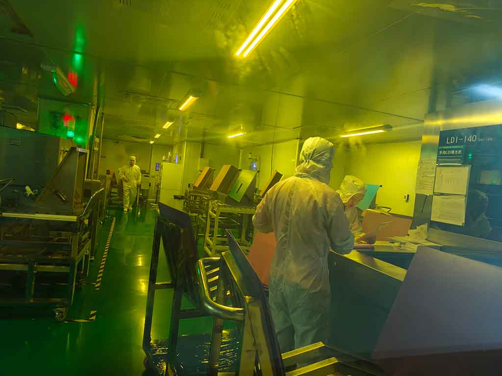
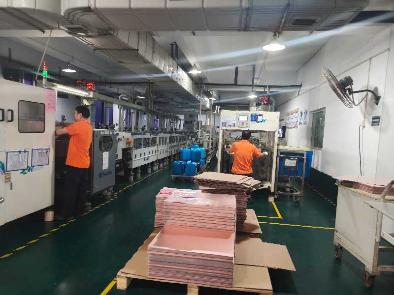
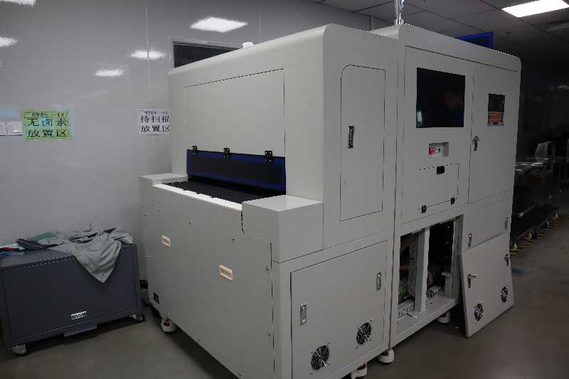
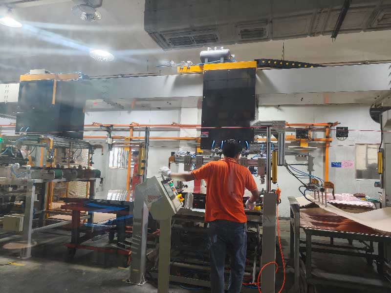
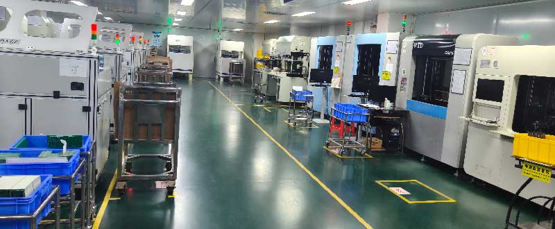
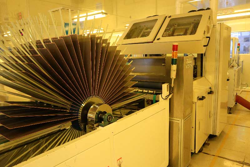
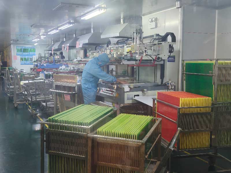
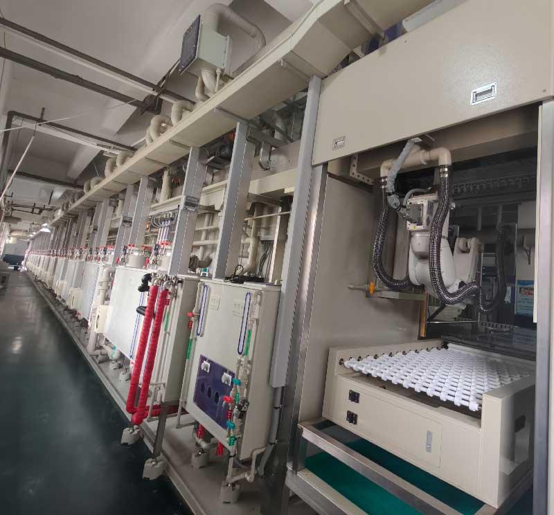
Our Facility
HXD has more than 15 years of PCB production experience. We continue to invest in advanced manufacturing and inspection equipment. Laser direct imaging systems, high-precision lamination presses, regular maintenance, and strict process control help deliver stable PCB quality.
Quality Assurance
We manufacture every PCB board through a structured quality process. This ranges from inner layer inspection to final board verification, ensuring your boards perform exactly as designed.
Every board is fully tested for open circuits, short circuits, and net continuity before shipment. We use flying probe or fixture-based testing depending on volume, ensuring zero electrical defects reach your assembly line.
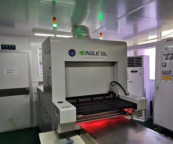
High-resolution AOI systems scan the inner and outer layers. They find trace defects, missing pads, solder mask misalignment, and other visual issues. This helps catch problems early, saving money.
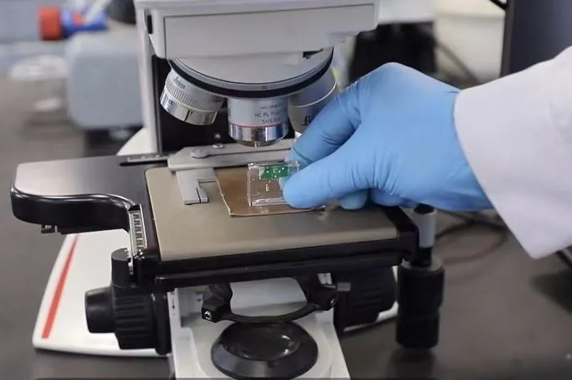
We use micro-sectioning to check the inside of the PCB. By cutting a small sample and viewing it under a microscope, we can inspect via plating, layer alignment, and bonding quality. This helps make sure every board is strong and reliable.
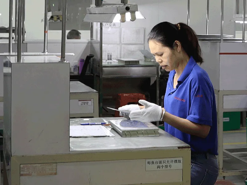
Before packaging, each board gets a detailed final inspection. We check dimensions, surface finish, hole quality, silkscreen accuracy, and overall workmanship. This all meets IPC Class 2 or Class 3 standards.
All quality records are traceable and available upon request. We stand behind every board we ship.