HXDcircuit

Rigid PCB Manufacturing for High-Quality Multi-Layer Boards

  • No MOQ
  • Rigid PCB up to 32Layers
  • HDI board with any layer
  • Special technology can be available: Half hole, Buried Copper Coin and etc
  • Wide Material Options Including High-End RF Laminates: ISOLA 370HR, Rogers 4350, F4BM255 – materials many suppliers cannot provide, with stable availability
  • IPC Class3 compliance, UL and ISO Certified

PCB Certifications

Multi-Layer Rigid PCBs

10Layer coil PCB with thick copper weight

10Layer coil PCB with thick copper weight

Designed specifically for high-power industrial applications, ensuring reliable performance under demanding conditions.

12Layer FR4 ISOLA 370HR Tg170

12Layer FR4 ISOLA 370HR Tg170

Reliable Supply of ISOLA 370HR (Tg170),Industrial-Grade 12-Layer Stack-Up,High-Precision Conductive Performance

12Layer HDI with ISOLA 370HR Tg170

12Layer HDI with ISOLA 370HR Tg170

12-layer stackup with multiple HDI build-up (L1-2, L11-12) enables high-density routing, compact layouts, and advanced miniaturized designs.

14Layer with FR4 Tg180

14Layer with FR4 Tg180

Designed for complex, high-speed broadcasting systems requiring multi-layer signal integrity and stable performance.

4Layer Rigid-flex PCB

4Layer Rigid-flex PCB

Stable 4-Layer Rigid-Flex Design (FR4 + PI) Combines flexibility and rigidity to support compact layouts and dynamic bending in industrial control applications.

4Layer Rogers4350+FR4 with Hybrid Laminating PCB

4Layer Rogers4350+FR4 with Hybrid Laminating PCB

Rogers 4350 for RF layers + FR4 for structural layers, delivering high-frequency performance with lower material cost

4layer with Half hole

4layer with Half hole

Edge-plated half holes enable module plug-in, board-to-board connection, and compact mechanical integration.

4Layer with Rogers+FR4 Hybrid Board+Copper Coin Buried

4Layer with Rogers+FR4 Hybrid Board+Copper Coin Buried

Hybrid Material: FR4 Tg170 + Rogers 4350,4-Layer Rigid Structure for Broadcasting Applications,High-Precision PCB Capability

mutiplayer-pcb

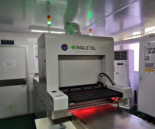
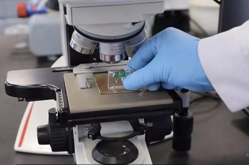
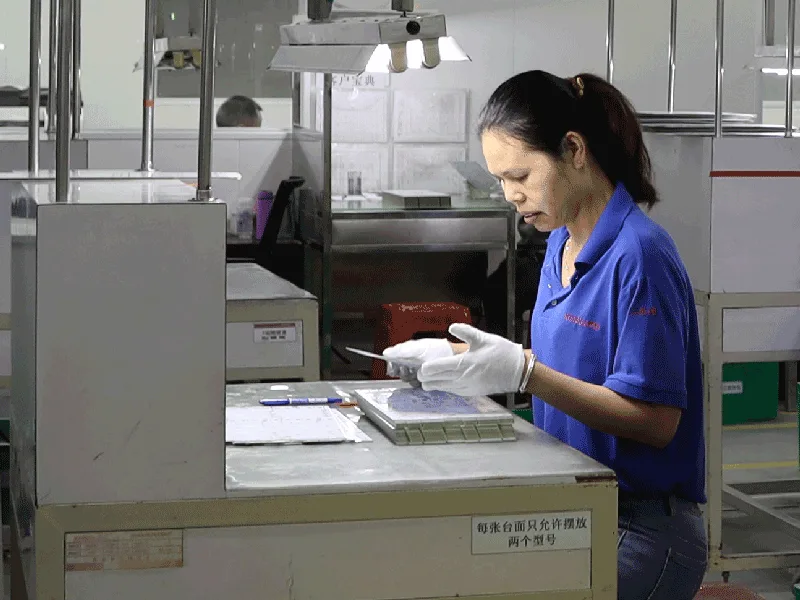
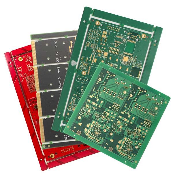
Different Types of Rigid PCB

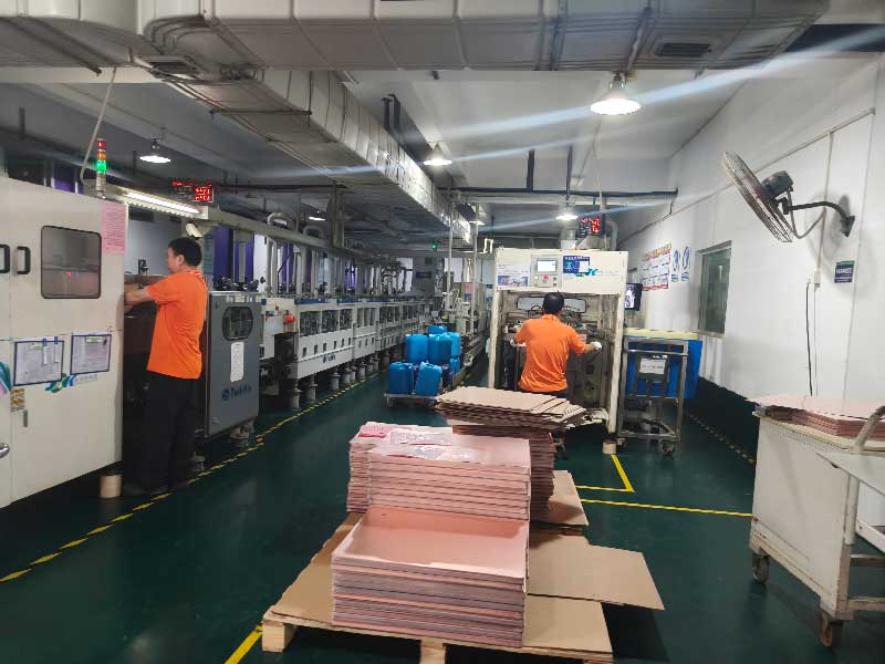
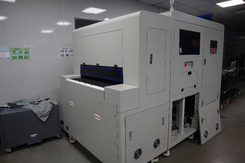
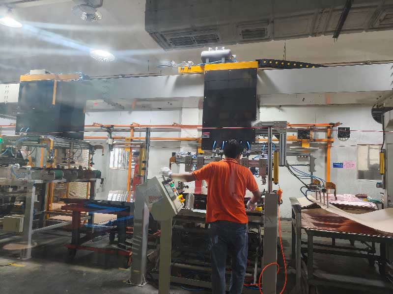
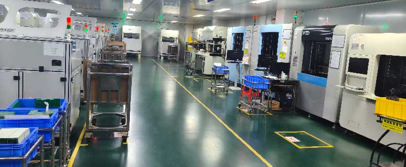
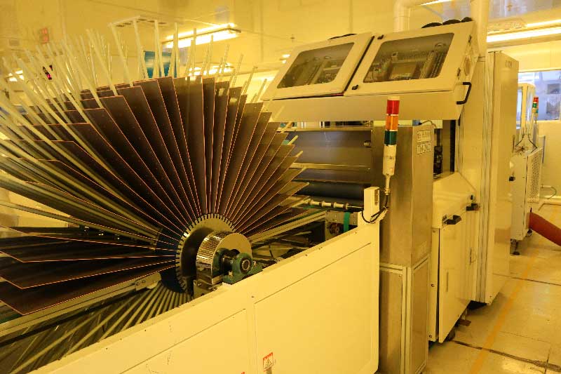
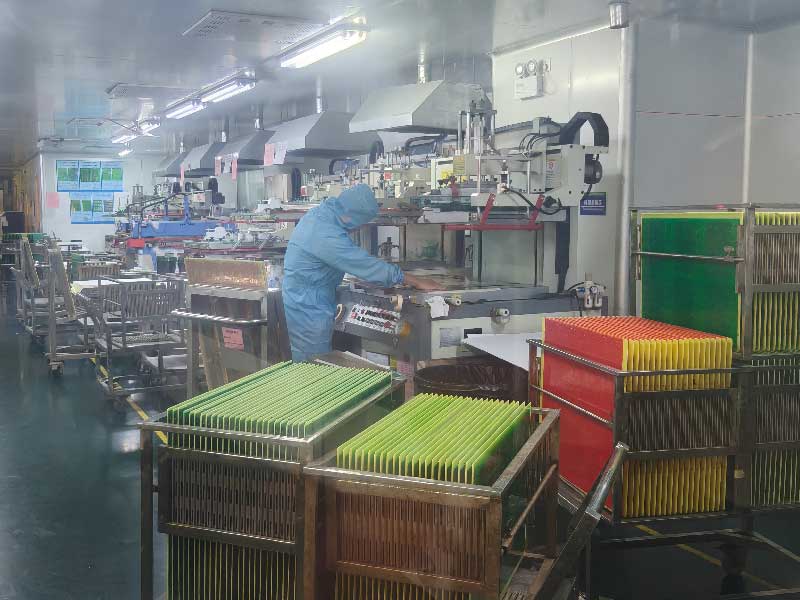
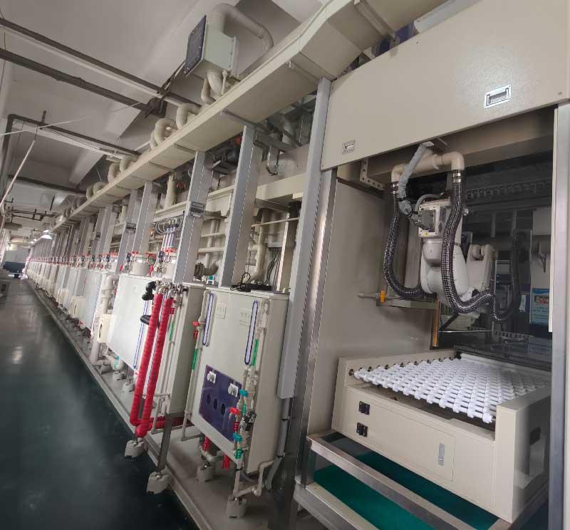
HXD can supply various rigid PCB types to meet the needs of different electronic applications:

Single-Sided PCB: A Single-Sided PCB has conductive traces on only one side of the substrate. It has a simple structure, and its production process is very mature. Because it uses fewer materials and fewer steps, it usually has the lowest production cost of common PCB types.

Double-Sided PCB:  A Double-Sided PCB has conductive circuits on both sides of the substrate. Electrical connections between the two sides are made through Plated Through Holes (PTH). Compared with a single-sided board, a double-sided PCB offers much higher wiring density. This allows designers to place more components and build more complex circuit layouts.

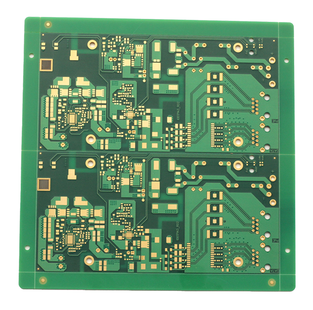
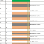
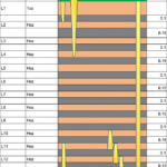
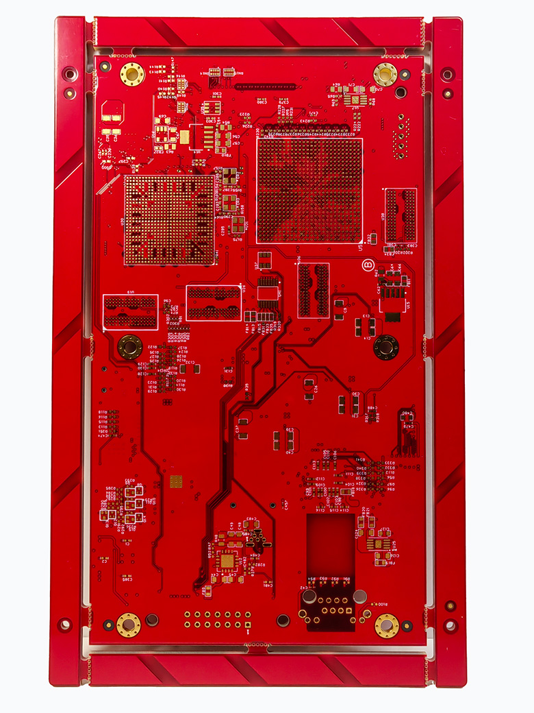
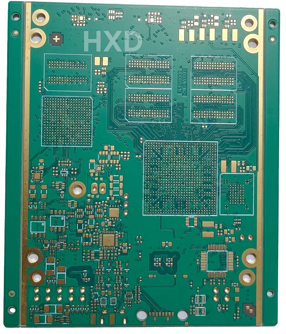
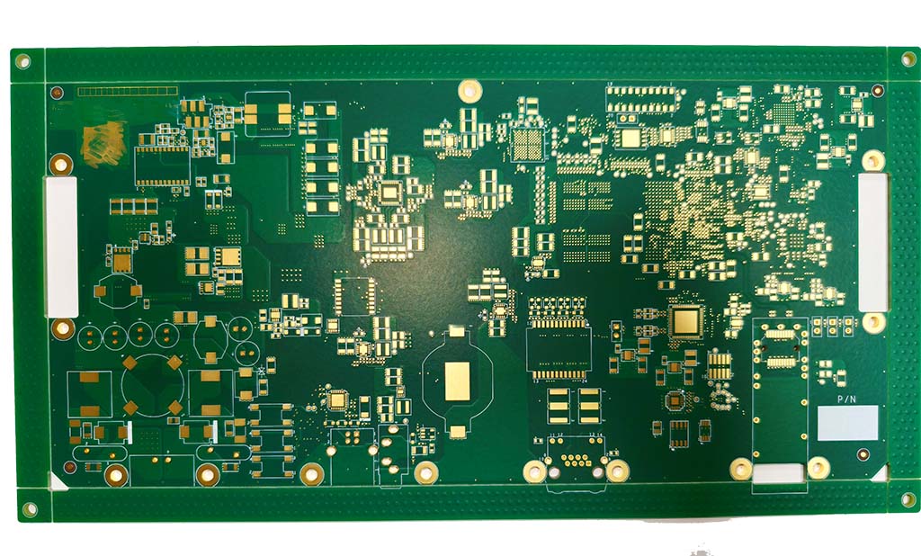
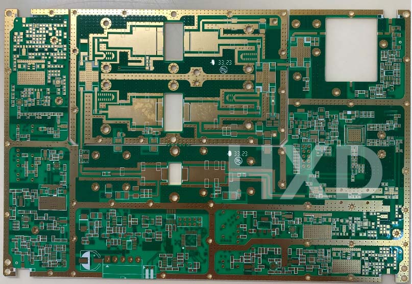
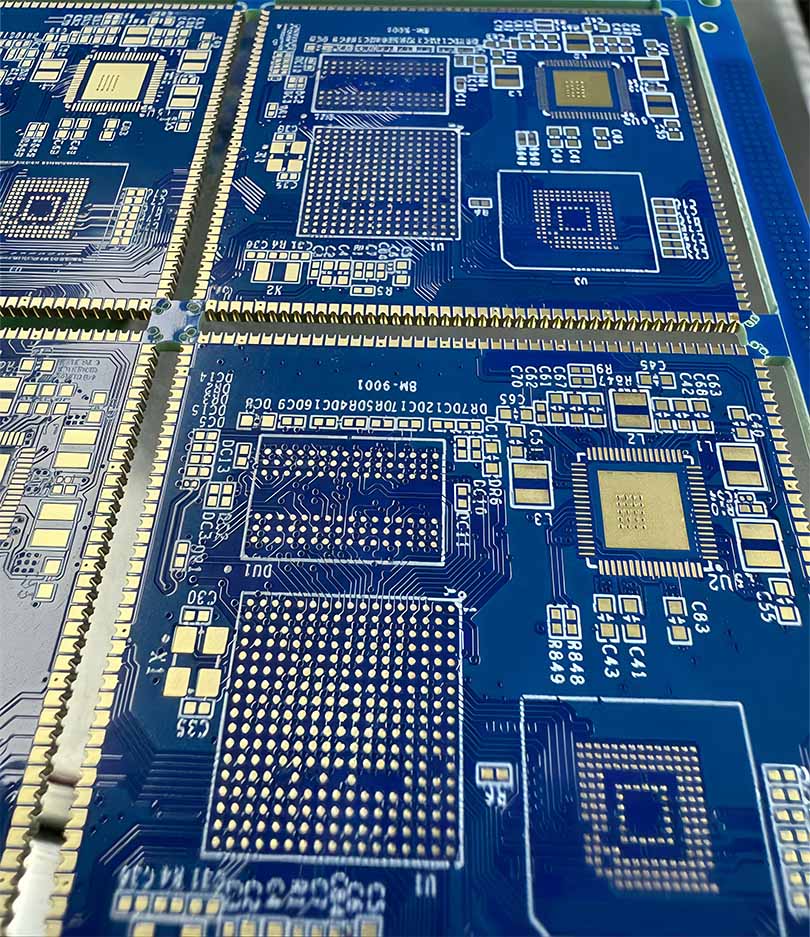
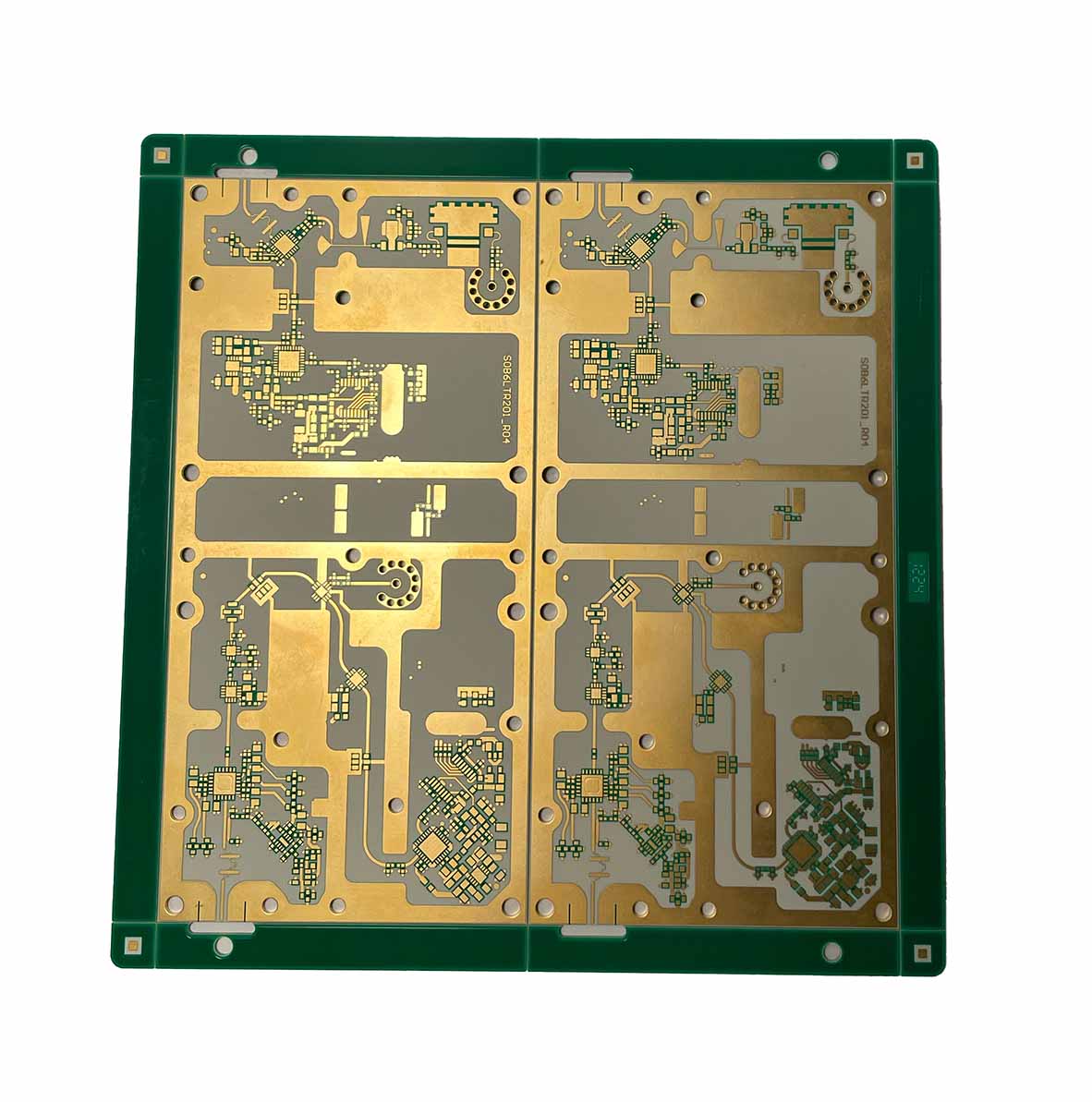
Multilayer PCB: Multilayer PCBs have three or more conductive layers separated by insulating materials. The layers are connected through vias,  blind vias, and buried vias. These boards are used in high-performance products that need more routing space, better signal control, and stable power delivery.

HXD provides custom multilayer PCB solutions, including 4-layer, 6-layer,  8-layer, and 10-layer PCBs. We can adjust the stackup, materials, copper thickness, vias, and surface finish based on your project requirements.

rigid-pcb

Why Choose HXD for Rigid PCB Manufacturing?

  • Advanced Capabilities: Specialized in multi-layer PCB and HDI PCB engineering and mass production.We have a mature  PCB manufacturing process.
  • Precision Control:  Strict management of lamination, plating, and etching to meet industrial and automotive standards.
  • Engineering Support:  We offer professional DFM reviews, stack-up optimization, and precise hole-size management.
  • Proven Reliability: Our boards are trusted in automotive electronics, industrial computers, and high-reliability systems.
  • Flexible Production: From rapid prototyping to high-volume fabrication, we help you get to market faster.

Rigid PCB Fabrication Capabilities

ItemsStandard PCBAdvanced PCB
Board TypeRigid 
Number of Layers1-20 layers50 Layers
MaterialFR-4, Aluminum, Copper Base, PTFE, Ceramic, Polyimide. Special material can be offered, such as Rogers, PTFE, ISOLA, Panasonic,Learn more about the materials we use in PCB manufacturing. 
Maximum PCB Size (Dimension)1L&2L: Min. 3×3mm Max: 600×1500mm
Multilayer: Min. 5×5mm Max: 600×1400mm
 
Board Size Tolerance (Outline)Min. ±0.1mm 
Board ThicknessMin. 0.15mm Max: 5.0mm 
Board Thickness Tolerance (t≥1.0mm)±10% 
Board Thickness Tolerance (t<1.0mm)±0.1mm 
Min Trace/SpacingMin. 2/2milMin. 1.5/1.5mil
Trace Width/Spacing Tolerance±20%±10%
Finished Copper ThicknessMin. 1/3oz, Max. 12oz 
Drill Sizes (CNC)Min. 0.15mmMin. 0.1mm
Drill Sizes (Laser)Min. 0.1mmMin. 0.05mm
Hole Location Accuracy±3mil±2mil
Max. Aspect Ratio16:120:1
Min Width of Annular Ring0.15mm (6mil) 
Finished Hole Size Tolerance (CNC)PTH: ±0.075mm, NPTH: ±0.05mmPress Fit: ±0.05mm
Minimum Legend Width (Legend)0.15mm 
Legend Width to Height Ratio (Legend)1:05 
Minimum Diameter of Plated Half Holes0.4mm 
Surface FinishingHASL with lead, HASL lead-free, ENIG, OSP, Hard Gold, Immersion Silver, Immersion Tin, ENEPIG, Carbon Ink 
Solder Mask ColourGreen, Red, Yellow, Blue, White, Black, Matt Green, Matte Black, Purple, None 
SilkscreenWhite, Black, Yellow, None 
PanelizationV-cut, Jump V-cut, Routing 
TestAOI, Fly Probe Testing (Free), Ionic Test, E-test, Impedance Control 
CertificationISO9001, TS16949, ISO14001, UL, RoHS 
PCB Manufacturing

Ready to start your PCB project?

pload your Gerber files today and our engineering team will review your design and provide a competitive quote within hours.

Quote within 2 hours DFM review included IPC-A-600 certified

Rigid PCB Stackup

hxd-12-layer-pcb-stackup

HXD 12-Layer PCB Stack-up

Stack-up design is critical for reducing EMI and ensuring signal integrity. Our engineering team works closely with you to optimize layer counts and material combinations. We aim to provide the most cost-effective solution for mass production without compromising performance.

HXD Technical Advantages:

  • Precision Impedance Control: Using advanced lamination monitoring and high-precision etching, we control the thickness of Cores and Prepregs at the micron level. This ensures we meet impedance tolerance requirements of ±5% to ±10%.
  • Hybrid Lamination: We specialize in mixing materials like Rogers + FR4. By precisely controlling the Coefficient of Thermal Expansion (CTE) for different materials, we deliver high-frequency performance while significantly reducing your material costs.
  • Complex Interconnect Support: We provide expert stack-up designs for 10-layer and 12-layer HDI boards, fully supporting Blind and Buried Vias.

Example: 14-Layer Rigid-HDI PCB Stackup

14-layer-rigid-hdi-pcb-stackup

Finished Board Thickness: 1.6+/-10%mm
Application: Broadcasting
Layer: 14L
Special Feature: Resin Plugging
Impedance Tolerance Layer Reference Width/spacing mil(mm)
single ended impedance lines 50ohm ±10% L1, L14 L2, L13 6.0 (0.152)
differential impedance pairs 100ohm ±10% L1, L14 L2, L13 5.0 (0.127) / 9.0 (0.229)
differential impedance pairs 90ohm ±10% L1, L14 L2, L13 5.6 (0.142) / 6.4 (0.163)
single ended impedance lines 50ohm ±10% L3, L5, L10, L12 L2 + L4,
L4 + L6,
L9 + L11,
L11 + L13
4.0 (0.102)
single ended impedance lines 40ohm ±10% 5.4 (0.137)
differential impedance pairs 80ohm ±10% 4.7 (0.119) / 5.3 (0.135)
differential impedance pairs 90ohm ±10% 4.0 (0.102) / 5.0 (0.127)
differential impedance pairs 100ohm ±10% 4.0 (0.102) / 8.0 (0.203)

Example: 12-Layer Rigid PCB Stackup

hxd-12-layer-pcb-stackup

Finished Board Thickness: 1.6+/-10%mm
Application: Industry Control
Layer: 12L
Material: ISOLA 370HR
Min.Line W/S: 0.067/0.175mm
Surface Finish: ENIG
Special Feature: Resin Plugging+Impedance Control
Impedance Tolerance Layer Reference Width/Spacing (mm)
Single ended impedance lines 50Ω ±10% L1 L2 0.1
Differential impedance pairs 100Ω ±10% L1 L2 0.1/0.175
Single ended impedance lines 50Ω ±10% L3 L2/L4 0.086
Differential impedance pairs 100Ω ±10% L3 L2/L4 0.08/0.195
Single ended impedance lines 50Ω ±10% L5 L4/L6 0.07
Differential impedance pairs 100Ω ±10% L5 L4/L6 0.067/0.2
Single ended impedance lines 50Ω ±10% L8 L9/L7 0.086
Differential impedance pairs 100Ω ±10% L8 L9/L7 0.067/0.2
Single ended impedance lines 50Ω ±10% L10 L9/L11 0.086
Differential impedance pairs 100Ω ±10% L10 L9/L11 0.08/0.195
Single ended impedance lines 50Ω ±10% L12 L11 0.1
Differential impedance pairs 100Ω ±10% L12 L11 0.1/0.175

Advanced Equipment for Rigid PCB Manufacturing

HXD has more than 15 years of experience in multilayer PCB production. We keep investing in the latest manufacturing and inspection machines. We keep our equipment in great shape, including laser direct imaging and high-precision lamination presses. This ensures your boards are perfect every time.

LDI Exposure

LDI Exposure

Etching

Etching

pcb-Inner-AOI

Inner AOI

Innerlayer-Laminating

Innerlayer Laminating

pcb-E-test

E-test

Automatic-Dry-Film-Laminator

Automatic Dry Film Laminator

Semi-Auto-Legend-Printing

Semi Auto Legend Printing

VCP-Plating

VCP Plating

20+
Years Manufacturing Experience
50+
Advanced Production Machines
3,000㎡
Clean-Room Production Area
ISO
9001 · UL · IPC Certified

Quality Assurance

Quality Control and Testing for Rigid PCB

Each rigid PCB order goes through strict process control and inspection, from inner layer checks to final board verification. This helps ensure stable quality and reliable performance.

100% Electrical Testing

100% Electrical Testing

Every board is fully tested for open circuits, short circuits, and net continuity before shipment. We use flying probe or fixture-based testing depending on volume, ensuring zero electrical defects reach your assembly line.

100% Automated Optical Inspection

100% Automated Optical Inspection

High-resolution AOI systems scan the inner and outer layers. They find trace defects, missing pads, solder mask misalignment, and other visual issues. This helps catch problems early, saving money.

100% Micro-sectioning TEST

100% Micro-sectioning TEST

We use micro-sectioning to check the inside of the PCB. By cutting a small sample and viewing it under a microscope, we can inspect via plating, layer alignment, and bonding quality. This helps make sure every board is strong and reliable.

100% Final Quality Control (FQC)

100% Final Quality Control (FQC)

Before packaging, each board gets a detailed final inspection. We check dimensions, surface finish, hole quality, silkscreen accuracy, and overall workmanship. This all meets IPC Class 2 or Class 3 standards.

All quality records are traceable and available upon request. We stand behind every board we ship.

Rigid PCB Frequently Asked Questions

How many layers can a rigid PCB have?
A rigid PCB can have single layer, 2 layers, or multiple layers. Simple products often use single-sided or double-sided rigid PCBs. More complex designs may use 4-layer, 6-layer, 8-layer, 10-layer, or higher-layer boards. HXD supports custom rigid PCB manufacturing up to 32 layers, depending on design needs and manufacturing requirements.
What materials are used for rigid PCBs?
Common rigid PCB materials include standard FR-4, High-Tg FR-4, Rogers, PTFE, aluminum base, and copper base materials. FR-4 is used for most standard electronics. High-Tg FR-4 offers better heat resistance. Rogers and PTFE are used for RF and high-frequency designs. Aluminum and copper base materials help improve heat dissipation.
Can rigid PCBs support controlled impedance?
Yes. Controlled impedance is often required for high-speed signals, such as USB, PCIe, Ethernet, DDR, and RF circuits. Final impedance values should be confirmed with the PCB manufacturer before production.
What surface finishes are available for rigid PCBs?
Common surface finishes for rigid PCBs include HASL, lead-free HASL, ENIG, OSP, immersion silver, and immersion tin. ENIG is often used for high-density designs, while HASL is common for standard and cost-sensitive PCB projects.
Are rigid PCBs suitable for high-speed designs?
Yes. Rigid PCBs are widely used in high-speed electronic products. With the right stackup, material, impedance control, and reference plane design, rigid PCBs can support high-speed signals and reduce EMI. For advanced designs, materials such as High-Tg FR-4, low-loss laminates, Rogers, or hybrid stackups may be used.
What files are needed for rigid PCB manufacturing?
For rigid PCB manufacturing, you usually need Gerber files and drill files.
You also need stackup information, board thickness, and copper thickness.
Include surface finish, solder mask color, and quantity.
For controlled impedance boards, impedance requirements and trace width details should also be provided. Assembly projects may also need BOM and pick-and-place files.
Can HXD provide custom stackup support?
Yes. HXD can provide custom stackup support for rigid PCB projects. We can help review layer count, material selection, core and prepreg thickness, copper weight, impedance targets, and via structure. This helps improve manufacturability and reduce design risks before production.
What is the typical lead time for rigid PCB production?
The lead time for rigid PCB production depends on layer count, board complexity, materials, surface finish, quantity, and testing requirements. Simple rigid PCBs usually have shorter lead times. High-layer, HDI, controlled impedance, or special material boards may need more production time. Contact HXD with your files for an accurate lead time.
REQUEST A QUOTE

Supported file formats: PDF, DOC, DOCX, TXT, JPG, PNG (Max 2MB)