HXDcircuit

10-Layer PCB Manufacturing

HXD provides advanced 10-layer PCB manufacturing with ISO & UL certification, ensuring stable quality for high-complexity multilayer projects.

PCB Certifications

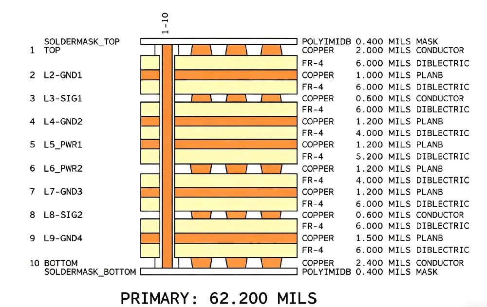
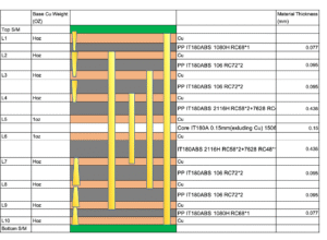
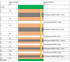
What is a 10-Layer PCB?

A 10-layer PCB  is a board made of 10 conductive copper layers stacked together. These layers are separated by insulating materials and connected through vias. It is used to build complex electronic circuits in a compact space.

A typical 10-layer PCB has 6 signal layers and 4 plane layers (power and ground). Signal layers (Signal) and plane layers (GND/PWR) are often arranged alternately. A 10-layer PCB is a high-end solution. It supports complex systems and handles high-speed signals and dense components.

Real-World References

10-Layer PCB Stackup Examples

Real stackup configurations from HXDcircuit production orders — use these as a reference when specifying your 10-layer PCB material and surface finish.

10-Layer PCB Stackup Example 1

Finished Board Thickness: 1.6+/-2%mm
Min. Line Width / Spacing 5/5 mil
Material: FR4 TU872 SLK
Surface Finish: Immersion Gold
Certification IPC-6012E Class II


No Imp Type Ctrl Up Ref Dn Ref Trace W Trace S IMP_Req
1 Single-ended L1 L3 10 75
2 Single-ended L1 L2 10 50
3 Differential L1 L2 6 6 100
4 Single-ended L3 L2 L4 6 50
5 Differential L3 L2 L4 5 7.5 100
6 Single-ended L8 L7 L9 6 50
7 Differential L8 L7 L9 5 7.5 100
8 Single-ended L10 L8 10 75
9 Single-ended L10 L9 10 50
10 Differential L10 L9 6 6 100

This 10-Layer stackup is used for industrial control. It uses FR-4 material with 4 ground planes and 2 dedicated power planes.The multi-ground design offers strong EMI shielding, stable power delivery, and clean signal routing.View product image.

10-Layer PCB Stackup example 2

10-layer-hdi-pcb-stackup

Finished Board Thickness: 1.9+/-10%mm
Application: Mobile Devices
Layer: 10L
Material: IT180A
Surface Finish: ENIG
Item Impedance Tolerance Layer Reference Width/spacing (mm)
1 single ended impedance lines 50ohm ±10% L1 L2 0.12
2 differential impedance pairs 100ohm ±10% L1 L2 0.1/0.25
3 single ended impedance lines 50ohm ±10% L3 L2/L4 0.125
4 differential impedance pairs 100ohm ±10% L3 L2/L4 0.075/0.175
5 single ended impedance lines 50ohm ±10% L5 L4/L6 0.165
6 differential impedance pairs 100ohm ±10% L5 L4/L6 0.112/0.175
7 single ended impedance lines 50ohm ±10% L8 L9/L7 0.082
8 differential impedance pairs 100ohm ±10% L8 L9/L7 0.075/0.175
9 single ended impedance lines 50ohm ±10% L10 L9 0.12
10 differential impedance pairs 100ohm ±10% L10 L9 0.104/0.246

Micro-section for Hole and surface copper thickness:View Detail

10-Layer PCB Stackup example 3

10-layer-pcb-stackup

Finished Board Thickness: 1.6+/-10%mm
Application: Broadcasting
Layer: 10L
Material: Panasonic M6
Surface Finish: ENIG
Min.Line W/S: 0.2/0.2mm
Special Feature: Impedance Control
Item Impedance Tolerance Layer Reference Width/spacing (mm)
1 single ended impedance lines
50ohm
±10% L1 L2 0.284
2 differential impedance pairs
100ohm
±10% L1 L2 0.16/0.14
3 single ended impedance lines
50ohm
±10% L1 L3 0.3
4 single ended impedance lines
50ohm
±10% L3 L2/L4 0.16
5 differential impedance pairs
100ohm
±10% L3 L2/L4 0.15/0.173
6 single ended impedance lines
50ohm
±10% L8 L9/L7 0.16
7 differential impedance pairs
100ohm
±10% L8 L9/L7 0.15/0.173
8 single ended impedance lines
50ohm
±10% L10 L9 0.28
9 single ended impedance lines
50ohm
±10% L10 L8 0.3
10 differential impedance pairs
100ohm
±10% L10 L9 0.16/0.14

Micro-section for Hole and surface copper thickness:View Details

Technical Specs

10-Layer PCB Manufacturing Capabilities

Explore our advanced processes, material options, and precision control for reliable 10-layer PCB production.

Items Standard PCB Advanced PCB
Copper Foil Thickness 12μm, 18μm, 35μm, 70μm, 105μm, 140μm (1/3oz – 4oz) 10oz
Max. Panel Size 24 × 28.5″ (622mm × 723mm) 24 × 40″ (622mm × 1000mm)
Laminate Materials FR-4, CEM-3, Mid Tg, High Tg, High CTI, Halogen Free /
Min. Inner Thin Core Thickness 3mil (0.075mm) /
Min. Inner Line Width / Spacing 2.5 / 3.5 mil (0.0635 / 0.089mm) 2.5 / 2.5 mil (0.0635mm)
Min. Outer Line Width / Spacing 3.5 / 3.5 mil (0.089 / 0.089mm) 3.0 / 3.0 mil (0.075 / 0.075mm)
Layer-to-Layer Registration Tolerance ±3mil (±0.075mm) /
Min. Finished Hole Size 0.2mm 0.15mm
Min. Drilling Bit Size 0.2mm /
Max. Drilling Bit Size 6.5mm /
Finished Hole Size Tolerance (PTH) ±0.075mm (±3mil) ±0.05mm (±2mil)
Drilling Precision Tolerance (vs CAD data) ±0.075mm (±3mil) ±0.05mm (±2mil)
PTH Hole Copper Thickness 20–30μm 10–15μm
Max. Aspect Ratio ≤ 10:1 12:1
Min. Solder Mask Opening 0.05mm (2mil) 0.02mm (0.8mil)
Min. Solder Dam 0.076mm (3mil) 0.063mm (2.5mil)
Surface Finish OSP, Peelable Solder Mask, Carbon Ink, HASL (lead free), ENIG, I-Ag, I-Tin OSP, Peelable Solder Mask, Carbon Ink, HASL (lead free), ENIG, I-Ag, I-Tin
OSP Thickness 0.2–0.5μm /
V-Cut Angle 20°, 30°, 45°, 60° /
Min. V-Cut Co-thickness 0.25mm /
Profiling Mode Routing & Punching /
Dimensional Tolerance ±0.10mm (4mil) /
E-Test Voltage 250 ± 5V /
Max. E/T Insulation Resistance 100 MΩ /
Min. E/T Conductive Resistance 20 MΩ /
Get a Quote

Get a Fast Quote for Your 10-Layer PCB

Send us your Gerber files today. Our team will review your project and provide a fast, accurate quote with reliable manufacturing support.

Quote within 2 hours DFM review included IPC-A-600 certified

Advanced Equipment for 10-Layer PCB Manufacturing

Manufacturing a 10-layer PCB is a highly complex process and much more challenging than producing 2-layer or 4-layer boards. HXD has many years of experience and a mature manufacturing system in the 10-layer PCB field. We are also equipped with advanced production equipment, including laser direct imaging (LDI) systems and high-precision lamination presses. We ensure every PCB delivers consistent high quality and reliable performance.

X-ray Target Drilling

X-ray Target Drilling

PTH Plated Through-Hole-Production Line

PTH Plated Through-Hole-Production LineEtching

pcb-Inner-AOI

Inner AOI

OPE Punching Production Line

OPE Punching Production Line

PCB Chemical Pre-treatment Line

PCB Chemical Pre-treatment Line

Automatic-Dry-Film-Laminator

Automatic Dry Film Laminator

Semi-Auto-Legend-Printing

Semi Auto Legend Printing

VCP-Plating

VCP Plating

15+
Years Manufacturing Experience
50+
Advanced Production Machines
3,000㎡
Clean-Room Production Area
ISO
9001 · UL · IPC Certified

Quality Assurance

Quality Checks for 10-Layer PCB Production

We manufacture every 10-Layer PCB through a structured quality process. This ranges from inner layer inspection to final board verification, ensuring your boards perform exactly as designed.

100% Electrical Testing

100% Electrical Testing

Every board is fully tested for open circuits, short circuits, and net continuity before shipment. We use flying probe or fixture-based testing depending on volume, ensuring zero electrical defects reach your assembly line.

100% Automated Optical Inspection

100% Automated Optical Inspection

High-resolution AOI systems scan the inner and outer layers. They find trace defects, missing pads, solder mask misalignment, and other visual issues. This helps catch problems early, saving money.

100% Micro-sectioning TEST

100% Micro-sectioning TEST

We use micro-sectioning to check the inside of the PCB. By cutting a small sample and viewing it under a microscope, we can inspect via plating, layer alignment, and bonding quality. This helps make sure every board is strong and reliable.

100% Final Quality Control (FQC)

100% Final Quality Control (FQC)

Before packaging, each board gets a detailed final inspection. We check dimensions, surface finish, hole quality, silkscreen accuracy, and overall workmanship. This all meets IPC Class 2 or Class 3 standards.

All quality records are traceable and available upon request. We stand behind every board we ship.

10-Layer PCB FAQs

How thick is a 10-layer PCB?
The thickness of a 10-layer PCB is not fixed and mainly depends on stack-up design, copper weight, and material selection.

In most standard designs, a 10-layer PCB typically has a finished thickness ranging from 1.0 mm to 2.4 mm, with 1.6 mm being the most common industry standard.
How much does a 10-layer PCB cost?
The cost depends on board size, quantity, material, surface finish, and lead time. Generally, 10-layer PCBs cost more than 4 or 6-layer boards due to the added complexity in manufacturing.
What are the common applications of 10-layer PCBs?
10-layer PCBs are widely used in industrial control systems, telecom equipment, medical devices, automotive electronics, and high-performance computing.
What surface finishes are available for 10-layer PCBs?
Common surface finishes include HASL, ENIG, OSP, and ENEPIG. The right choice depends on your assembly process and reliability requirements.
How is impedance controlled in a 10-layer PCB?
Impedance is controlled by adjusting trace width, dielectric thickness, and material properties in the stack-up design. Proper layer arrangement ensures stable 50Ω single-ended or 100Ω differential impedance.
How do I choose the right stackup for a 10-layer PCB?
A good stackup balances signal layers, power planes, and ground planes. Working with an experienced manufacturer like HXD ensures your stackup meets your signal integrity and EMI requirements.
REQUEST A QUOTE

Supported file formats: PDF, DOC, DOCX, TXT, JPG, PNG (Max 2MB)