
Automated Optical Inspection (AOI) for PCB Assembly
 steve ran
January 27, 2026
steve ran
January 27, 2026
Think Deeper with AI:


A PCB assembly can contain thousands of solder joints and many small components. Inspecting every detail by eye is slow, and difficult to scale.
Automated optical inspection solves this problem using controlled lighting, cameras, and software. It checks each board against defined criteria.
This guide explains what AOI is, describes how it works, identifies when you need 3D AOI, and lists what you should check before ordering PCB assembly.
What Is Automated Optical Inspection?
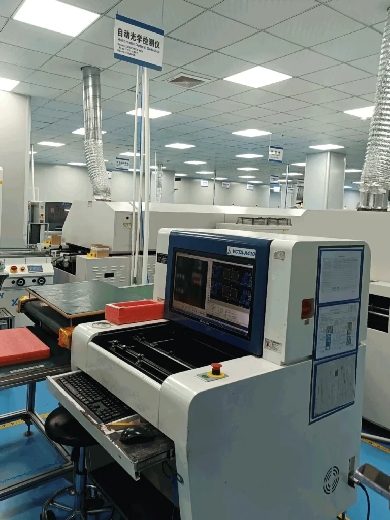
Automated optical inspection (AOI) is a machine-vision process used to inspect printed circuit boards and PCB assemblies. The system illuminates a board, captures images, analyzes visible features, and flags results that fall outside programmed limits.
During inspection, the AOI system captures and analyzes images of the PCB without electrically probing or powering the circuit. It checks the appearance, position, dimensions, markings, and visible solder features of the assembly.
Manufacturers can use optical inspection at several stages:
- During bare PCB production to inspect traces, pads, spacing, and copper features
- After component placement to check presence, position, and orientation
- After reflow soldering to examine visible joints and placement defects
- After through-hole or selective soldering when the system can view the target joints
Bare-board AOI uses similar imaging principles.
But its inspection program and defect library differ from those for populated boards.
Why AOI Matters in PCB Assembly
Smaller components and denser PCB layouts make manual inspection more difficult. AOI inspects every board using the same criteria, improving inspection consistency.
The main benefits include:
1. Earlier defect detection. Post-reflow AOI can identify visible defects before testing, final assembly, or shipment adds more cost.
2. Consistent inspection. A validated program applies defined limits across the production lot.
3. Faster feedback. Repeated defects can point to stencil, placement, feeder, reflow, or design problems.
4. Full-board coverage. Inline systems can inspect every board without relying only on sampling.
AOI does more than identify defective boards. It also helps engineers find process issues. For example, if components keep shifting, it may mean there is a placement problem. If solder bridges keep happening, the cause may be the solder paste, the pad design, or the reflow process.
How Does an AOI Inspection Machine Work?
An AOI inspection machine follows a controlled sequence:
- PCB enters the inspection area
- Controlled lighting illuminates the board
- One or more cameras capture images
- Software locates components and solder features
- Measurements are compared with programmed criteria
- Suspect features are flagged for review
- The board is accepted, rejected, or sent for verification
1. Program creation
The manufacturer first creates an inspection program for the assembly. The program may use CAD data, centroid data, the bill of materials, and package libraries. It may also use reference images and a verified first article. Operators define the features to inspect and the acceptable limits for each feature.
A “golden board” can provide a useful visual reference, but a known-good image should not be the only source of truth. A single sample may contain acceptable variation that does not represent the full process. Strong programs combine design data, measured limits, and verified production samples.
2. Controlled Lighting
AOI systems use LEDs with different colors, angles, and intensities. Light reflected from a flat pad looks different from light reflected from a curved solder fillet or raised lead. Multi-angle lighting makes edges, markings, polarity indicators, and solder shapes easier to classify.
3. Image capture
The camera records high-resolution images of the inspection area. Some machines use a top-down camera, while others add angled cameras for side views. The required optical resolution depends on the smallest feature, component pitch, board density, and inspection goal.
4. Image analysis
Software finds each component and compares its visible features with the inspection program. The AOI system locates each component and compares it with the inspection program to identify visible defects.
5. Defect Review
The system flags features that exceed the set limits. A trained operator then reviews uncertain results. This review matters because an AOI “call” is not always a true defect. Component color, reflective solder, board warpage, silkscreen variation, or lighting can create false calls.
Main Components of an AOI Inspection Machine
An AOI system combines optics, motion control, computing, and material handling.
| Component | Function |
|---|---|
| Camera or Camera Array | Captures images of components, markings, pads, and visible solder joints. |
| Lens and Optics | Controls magnification, field of view, focus, and image quality. |
| LED Lighting | Highlights edges, shapes, polarity marks, and solder joint geometry. |
| Motion System | Moves the camera or PCB to each inspection position. |
| Conveyor | Transfers PCBs through the SMT production line. |
| Processing Software | Analyzes images, measures features, and classifies inspection results. |
| Program and Component Library | Stores component data, reference images, and inspection criteria. |
| Review Station | Allows operators to verify defects and record inspection results. |
2D AOI vs 3D AOI Systems
Two-dimensional AOI evaluates features in a flat image. Three-dimensional AOI adds height or surface-profile data. The added Z-axis information makes 3D AOI useful when a defect depends on vertical geometry.
| Feature | 2D AOI | 3D AOI |
|---|---|---|
| Component Presence | Strong | Strong |
| X-Y Placement & Rotation | Strong | Strong |
| Polarity & Marking Check | Strong | Strong |
| Solder Bridge Detection | Good (Visible Joints) | Good (Visible Joints) |
| Height Measurement | No | Yes |
| Lifted Lead Detection | Limited | Better |
| Tombstone Detection | Good | Better |
| Solder Volume / Shape | Estimated | Measured |
| Dense Board Inspection | More Shadowing | Less Shadowing |
| Cost | Lower | Higher |
3D AOI does not make X-ray inspection unnecessary. Optical systems still need a line of sight. Solder balls under a BGA, voids under a bottom-terminated component, and other hidden parts need X-ray inspection.
Choose 3D AOI for complex PCB assemblies with fine-pitch or mixed-height components. For simpler boards with clear visible features, 2D AOI is often sufficient.
AOI vs SPI vs X-Ray Inspection
SPI, AOI, and X-ray serve different purposes and work best together.
| Inspection Method | Typical Production Point | Main Purpose | Common Findings |
|---|---|---|---|
| SPI | After Solder Paste Printing | Check solder paste deposition before component placement. | Missing, excess, offset, insufficient, or bridged solder paste. |
| Pre-Reflow AOI | After Placement, Before Reflow | Verify component placement before soldering. | Missing, incorrect, shifted, rotated, or reversed components. |
| Post-Reflow AOI | After Reflow | Inspect visible solder joints and component placement. | Bridges, tombstones, lifted leads, and other visible solder defects. |
| X-ray / AXI | After Reflow | Inspect hidden solder joints and internal connections. | BGA bridges, voids, head-in-pillow, hidden opens, and barrel fill. |
| ICT / Flying Probe | After Assembly | Verify electrical connections and component values. | Opens, shorts, incorrect values, and some device faults. |
| Functional Test | End of Production | Verify overall product functionality. | Firmware, interface, performance, and system-level faults. |
SPI catches paste problems before components and reflow make repair more expensive. AOI checks visible assembly features. X-ray examines hidden joints. Electrical and functional tests confirm conditions that cameras cannot prove.
No single inspection method provides complete coverage. The correct test plan depends on package mix, product risk, production volume, access, and customer requirements.
Where AOI Fits in the SMT Assembly Process
A common SMT quality flow looks like this:
- 1.Solder paste printing
- 2.SPI
- 3.Pick and place
- 4.Optional pre-reflow AOI
- 5.Reflow soldering
- 6.Post-reflow AOI
- 7.X-ray for hidden-joint packages as required
- 8.Repair and verification
- 9.Electrical and/or functional testing
- 10.Final inspection and shipment
Post-reflow AOI is the most common because it inspects finished solder joints. Pre-reflow AOI can detect placement issues before soldering on high-risk products.
For new-product introduction, engineers should review first-article results and tune the AOI program before volume production. Once production stabilizes, defect trends can reveal process drift and guide corrective action.
How Much Does AOI Inspection Cost?
In many contract manufacturing quotes, AOI is part of the assembly and quality control cost. It often does not appear as a separate line item.
The main cost drivers include:
Programming time: A new assembly needs data preparation, library setup, first-article verification, and threshold tuning.
Board complexity: More components, fine-pitch leads, dense layouts, and double-sided assembly increase inspection work.
Production volume: Setup cost spreads across more units in a longer run.
Inspection technology: 3D AOI and specialized optics cost more to own and operate than basic 2D systems.
Inline or offline workflow: Inline AOI works well for fast, high-volume production. Offline systems are more flexible. They are better for prototypes and mixed production.
Reporting and traceability: Stored images, serial-number linkage, detailed reports, and customer-specific records add data-handling requirements.
Additional coverage: SPI, X-ray, ICT, flying probe, and functional testing add separate processes.
To prepare an accurate quote, we need your Gerber or ODB++ files, BOM, centroid file, assembly drawing, expected production volume, and testing requirements.
Need a PCB assembly inspection plan for your next project?
Limitations of AOI
AOI is a visual inspection process, so its limits are clear.
AOI cannot see through components
The camera cannot directly inspect solder balls under BGAs. It also cannot see hidden joints under many QFN, LGA, and bottom-terminated packages. X-ray inspection provides better coverage for these features.
AOI cannot prove electrical function
A correct-looking joint may still have an electrical problem. A board may also contain a wrong-value unmarked component, damaged device, firmware issue, or design fault. Electrical and functional tests cover these risks.
AOI can generate false calls
Reflective solder, component color changes, board warpage, silkscreen variation, and inconsistent markings can trigger false alarms. A trained operator and a controlled program-review process remain necessary.
Inspection quality depends on the program
Expensive hardware cannot compensate for poor libraries, incorrect tolerances, weak first-article validation, or careless disposition of alarms. Buyers should evaluate the supplier’s process, not just the machine model.
Coverage depends on design and access
Tall parts can shadow smaller components. Closely spaced packages can block angled views. Design-for-inspection practices, clear polarity marks, accessible test points, and an early DFM review improve coverage.
How to Evaluate a PCB Assembly Supplier’s AOI Capability
Use this checklist during supplier evaluation:
- Can the supplier provide defect images or an inspection report when required?
- How does AOI data feed corrective action and process control?
- Which hidden-joint packages receive X-ray inspection?
- Which electrical or functional tests follow optical inspection?
- Which acceptance standard and product class apply to the order?
IPC-A-610 provides visual acceptance criteria for electronic assemblies. The required revision and product class should be confirmed before production.
Conclusion
Automated optical inspection gives PCB manufacturers a fast and repeatable way to find visible assembly defects.
Inspection methods should match the product’s requirements. SPI checks solder paste, AOI detects visible defects, X-ray inspects hidden solder joints, and electrical testing verifies circuit function.
FAQ
Frequently Asked Questions
What is the difference between CCD and AOI?
AOI is the complete automated inspection system. An AOI machine may use CCD or CMOS cameras together with lenses, lighting, motion control, inspection software, component libraries, and review tools.