HXDcircuit
PCB Manufacturing

4-Layer PCB Manufacturing

High-quality 4-layer PCBs built for signal integrity, stable performance, and scalable production. From quick-turn prototypes to volume orders, we help you ship faster with confidence.

4-Layer PCB Products

4Layer Rigid-flex PCB

4Layer Rigid-flex PCB

Stable 4-Layer Rigid-Flex Design (FR4 + PI) Combines flexibility and rigidity to support compact layouts and dynamic bending in industrial control applications.

4Layer Rogers4350+FR4 with Hybrid Laminating PCB

4Layer Rogers4350+FR4 with Hybrid Laminating PCB

Rogers 4350 for RF layers + FR4 for structural layers, delivering high-frequency performance with lower material cost

4Layer with Rogers+FR4 Hybrid Board+Copper Coin Buried

4Layer with Rogers+FR4 Hybrid Board+Copper Coin Buried

Hybrid Material: FR4 Tg170 + Rogers 4350,4-Layer Rigid Structure for Broadcasting Applications,High-Precision PCB Capability

4layer with Half hole

4layer with Half hole

Edge-plated half holes enable module plug-in, board-to-board connection, and compact mechanical integration.

PCB Certifications

Technical Specs

4-Layer PCB Manufacturing Capabilities

Comprehensive 4-layer PCB manufacturing capabilities covering stackup design, material selection, copper thickness options, and precision fabrication for diverse applications.

Items Standard PCB Advanced PCB
2 Finished Board Thickness 16~128 mil (0.4mm – 3.2mm) /
3 Max. Panel Size 24 × 28.5″ (622mm × 723mm) 24 × 40″ (622mm × 1000mm)
4 Laminate Materials FR-4, CEM-3, Mid Tg, High Tg, High CTI, Halogen Free /
5 Finished Board Thickness Tolerance < 1.0mm ±0.10mm (±4mil)
1.0~1.6mm ±0.15mm (±6mil)
< 1.0mm ±0.075mm (±3mil)
1.0~1.6mm ±0.10mm (±4mil)
6 Min. Inner Thin Core Thickness 3mil (0.075mm) /
7 Min. Inner Line Width / Spacing 2.5 / 3.5 mil (0.0635 / 0.089mm) 2.5 / 2.5 mil (0.0635mm)
8 Min. Outer Line Width / Spacing 3.5 / 3.5 mil (0.089 / 0.089mm) 3.0 / 3.0 mil (0.075 / 0.075mm)
9 Layer-to-Layer Registration Tolerance ±3mil (±0.075mm) /
10 Copper Foil Thickness 12μm, 18μm, 35μm, 70μm, 105μm, 140μm (1/3oz – 4oz) /
11 Min. Finished Hole Size 0.2mm 0.15mm
12 Min. Drilling Bit Size 0.2mm /
13 Max. Drilling Bit Size 6.5mm /
14 Finished Hole Size Tolerance (PTH) ±0.075mm (±3mil) ±0.05mm (±2mil)
15 Finished Hole Size Tolerance (NPTH) ±0.05mm (±2mil) /
16 Drilling Precision Tolerance (vs CAD data) ±0.075mm (±3mil) ±0.05mm (±2mil)
17 PTH Hole Copper Thickness 20–30μm 10–15μm
18 Max. Aspect Ratio ≤ 10:1 12:1
19 Impedance Control ±10% ±8%
20 Min. Solder Mask Opening 0.05mm (2mil) 0.02mm (0.8mil)
21 Min. Solder Dam 0.076mm (3mil) 0.063mm (2.5mil)
22 Surface Finish OSP, Peelable Solder Mask, Carbon Ink, HASL (lead free), ENIG, I-Ag, I-Tin OSP, Peelable Solder Mask, Carbon Ink, HASL (lead free), ENIG, I-Ag, I-Tin
23 OSP Thickness 0.2–0.5μm /
24 V-Cut Angle 20°, 30°, 45°, 60° /
25 Min. V-Cut Co-thickness 0.25mm /
26 Profiling Mode Routing & Punching /
27 Dimensional Tolerance ±0.10mm (4mil) /
28 E-Test Voltage 250 ± 5V /
29 Max. E/T Insulation Resistance 100 MΩ /
30 Min. E/T Conductive Resistance 20 MΩ /

In addition to 4-layer PCBs, we produce 6-layer PCB,  8-layer PCB, 10-layer PCB, and 12-layer PCB boards.These are ideal for complex and high-performance applications.

Get a Quote

Get instant pricing for your 4-layer PCB

Get high-quality 4-layer PCBs with fast turnaround, competitive pricing, and no MOQ — from single prototype builds to full-scale production.

Quote within 2 hours DFM review included IPC-A-600 certified

Real-World References

4-Layer PCB Stackup Examples

Real stackup configurations from HXDcircuit production orders — use these as a reference when specifying your 4-layer PCB material and surface finish.

4-Layer PCB Stackup Example 1

4-layer High Frequency Hybrid Rigid PCB Stackup


Finished Board Thickness: 1.0+/-10%mm
Material: Ro4350B(Tg>280)+IT180A
Surface Finish: ENIG
Type: High Frequency Hybrid Rigid PCB

This 4-layer hybrid PCB stackup is ideal for communication PCB applications. Rogers RO4350B helps reduce signal loss and supports stable RF performance. IT180A FR-4 improves board strength and keeps the cost under control. This stackup is suitable for wireless modules, antenna boards, RF front-end circuits, routers, and base station equipment. View Product Images.

4-Layer PCB Stackup Example 2

4-Layer PCB Stackup for High-Frequency Hybrid PCB + HDI

4-Layer PCB Stackup for High-Frequency Hybrid PCB + HDI

Finished Board Thickness: 1.2+/-10%mm
Application: Advanced Radar Systems
Material: Ro4350B+S1000-2
Surface Finish: ENIG
Special Feature: Buried Copper Coin, Resin plugging

This 4-layer hybrid PCB stackup is ideal for Radar PCB applications. It uses Rogers RO4350B to reduce signal loss and support stable RF signals. S1000-2M prepreg improves board strength and keeps cost under control. This stackup suits radar sensors, millimeter-wave modules, RF front-end boards, and high-frequency antenna circuits. View product images.

4-Layer Rigid-Flex PCB Stackup Example 3

Finished Board Thickness: 1.0+/-10%mm
Material:  AP8535R ,TG170
Surface Finish: ENIG
Special Feature: Buried Copper Coin, Resin plugging

This 4-layer rigid-flex PCB stackup uses a double-layer flexible core between L2 and L3, with FR4 rigid sections on both sides. The thin inner copper supports better bending performance, while the plated outer copper layers provide reliable assembly and interconnection.
This structure is suitable for compact electronics, wearable devices, medical equipment, sensors, and products that need stable flex-to-rigid connections. View product images.

What Is a 4-Layer PCB?

A 4-layer PCB is a printed circuit board with four conductive copper layers separated by insulating material. It usually includes two outer signal layers and two inner layers used for power and ground. This design offers more routing space, cleaner return paths, and improved signal integrity compared to a 2-layer board.

The standard 4 layer pcb stackup​ is Top Signal / GND Plane / Power Plane / Bottom Signal. It keeps signal layers on the outside, while the internal layers provide stable ground and power references.

Compared to 2-layer boards, 4-layer PCBs are widely used when products need higher circuit density, lower EMI, more stable power delivery, and better overall electrical performance.

4-Layer PCB Stackup Overview

  • Top Signal: Copper routing layer for key signals.
  • GND Plane: Continuous plane for return current.
  • Power Plane: Internal plane for power rails.
  • Bottom Signal: Secondary routing layer.
Layer Function Cross Section L1 L2 L3 Core L4 Top Signal GND Plane Power Plane FR4 Bottom Signal Signal layer Ground plane Power / copper layer FR4 core / prepreg

Overview

4-layer PCB Stackup Overview

There is no single 4-layer stackup that fits every product. Designers should choose the most suitable stackup based on specific needs, such as electrical performance, EMI control, power distribution, and routing requirements, the following stack-up are commonly used.

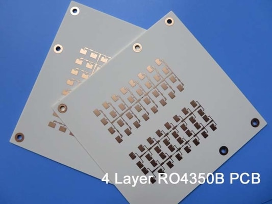
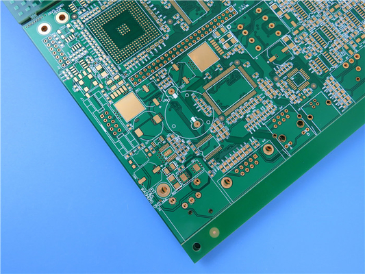
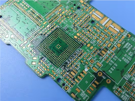
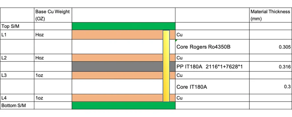
Signal – GND – PWR – Signal

This is the most widely used stackup structure. It offers a perfect balance between circuit complexity, manufacturing cost, and electrical performance. It is ideal for the following applications:IoT Devices 、 Sensors、Industrial Control 、 Automotive Electronics、Consumer Electronics

GND – Signal – Signal – GND

This structure stops outside interference from entering the circuit. It also keeps internal signals from leaking out. It’s often used in high-speed digital designs that are very sensitive to noise. However, it also presents some design challenges.

Signal – GND – GND – PWR

This is a power-focused structure. If your PCB is mainly designed to drive motors or handle high-power conversion with simple control logic, this structure is perfect. It provides a more stable power supply and a cleaner grounding environment than standard stack-up.

Key Benefits of 4-Layer PCB

4-layer PCBs improve electrical performance and routing flexibility while keeping production practical and cost-efficient.

Better Signal Integrity

In a 4-layer PCB, dedicated ground and power planes help reduce signal noise and crosstalk. This means a cleaner and more reliable signal. It’s better than single or double-sided boards.

Enhanced EMI Shielding

4-layer PCBs have inner ground planes that shield against EMI. This makes them great for high-frequency and high-speed applications.

Better Power Distribution

A dedicated power plane ensures stable voltage delivery across the entire board, reducing power fluctuations and improving overall circuit performance.

Thermal Management

The additional copper layers help dissipate heat more efficiently, extending component lifespan and improving reliability in high-power applications.

Higher Reliability

4-layer PCBs meet IPC Class II and Class III standards, making them suitable for demanding industries such as automotive, aerospace, medical, and industrial equipment.

A Cost-Effective Choice for Complex Circuits

A 4-layer PCB is much more powerful than a 2-layer board, but its manufacturing cost is significantly lower than 6 or 8-layer boards. This makes it the best choice for medium-complexity circuits.

Get a Quote

Ready to Start your 4-Layer PCB?

Upload your Gerber files today and our engineering team will review your design and provide a competitive quote within hours.

Quote within 2 hours DFM review included IPC-A-600 certified

Why Choose HXD for Your 4-Layer PCBs?

Submit before 9am and we start production the same day. No compromise on quality, ever.

Custom Stackup

We support standard and custom 4-layer stackup, ensuring optimal signal integrity and EMI shielding for your specific design requirements.

Full Range of Thickness

From 0.4mm to 3.2mm ,we manufacture any 4-layer PCB thickness to your exact specifications — no MOQ

Diverse Substrates

We offer Standard FR-4,High-Tg,Rogers,Ceramic, and Polyimide to meet all your thermal management needs.

Advanced Technology

Supports blind and buried vias, controlled impedance, via-in-pad, and back-drill techniques.

Surface Finishes

HASL Lead-Free, OSP, Immersion Silver, Immersion Tin, and Hard Gold.

Advanced Equipment for 4-Layer PCB Manufacturing

HXD has more than 15 years of experience in multilayer PCB production. We keep investing in the latest manufacturing and inspection machines. We keep our equipment in great shape, including laser direct imaging and high-precision lamination presses. This ensures your boards are perfect every time.

LDI Exposure

LDI Exposure

Etching

Etching

pcb-Inner-AOI

Inner AOI

Innerlayer-Laminating

Innerlayer Laminating

pcb-E-test

E-test

Automatic-Dry-Film-Laminator

Automatic Dry Film Laminator

Semi-Auto-Legend-Printing

Semi Auto Legend Printing

VCP-Plating

VCP Plating

15+
Years Manufacturing Experience
50+
Advanced Production Machines
3,000㎡
Clean-Room Production Area
ISO
9001 · UL · IPC Certified

Frequently Asked Questions About 4-Layer PCB

When Should I Use a 4-Layer PCB?
You need cleaner EMC behavior than a 2-layer board can usually deliver.

You have medium-to-high pin count devices with limited routing channels.

You need a dedicated ground plane and more stable power distribution.

You are routing moderate-speed digital or mixed-signal interfaces.

You want a strong cost/performance compromise before jumping to 6 layers.
What factors affect the cost of 4-layer PCB manufacturing?
The cost of 4-layer PCB manufacturing depends on several key factors:

Board Size: Larger boards require more materials, which leads to higher costs.

Surface Finish: For example, ENIG (Gold) is typically more expensive than HASL (Solder).

Design Complexity: Features like Blind and Buried Vias or Controlled Impedance requirements will increase manufacturing difficulty and cost.
Copper Thickness: Using heavy copper (such as 2oz) will add to the total price.
What is the standard thickness for a 4-layer PCB?
The most common thickness for a 4-layer PCB is 1.6 mm. Other options are also available, such as 0.8 mm for mobile devices, and 1.2 mm or 2.0 mm for special needs.

We offer PCB board thickness ranging from 0.4 mm to 3.2 mm.
Is a 4-layer PCB much more expensive than a 2-layer PCB?
It costs more than 2-layer, but often reduces redesign risk and improves reliability, making total project cost more efficient.
REQUEST A QUOTE

Supported file formats: PDF, DOC, DOCX, TXT, JPG, PNG (Max 2MB)