PCB Certifications


Standard 2-Layer PCB Options
| Product | 2 Layer 1.6 mm 35 µm HASL | 2 Layer 1.6 mm 35 µm ENIG |
|---|---|---|
| Stackup | variable | variable |
| Layers | 2 | 2 |
| Surface finish | HASL | ENIG |
| Base material | FR4 TG 140°C | FR4 TG 140°C |
| PCB Thickness | 1.6 mm (63mil) | 1.6 mm (63mil) |
| Copper thickness | 35µm | 35µm |
| Product | 2 Layer 1.6 mm 70 µm HASL | 2 Layer 1.6 mm 70 µm ENIG |
|---|---|---|
| Stackup | variable | variable |
| Layers | 2 | 2 |
| Surface finish | HASL | ENIG |
| Base material | FR4 TG 140°C | FR4 TG 140°C |
| PCB Thickness | 1.6 mm (63mil) | 1.6 mm (63mil) |
| Copper thickness | 70µm | 70µm |
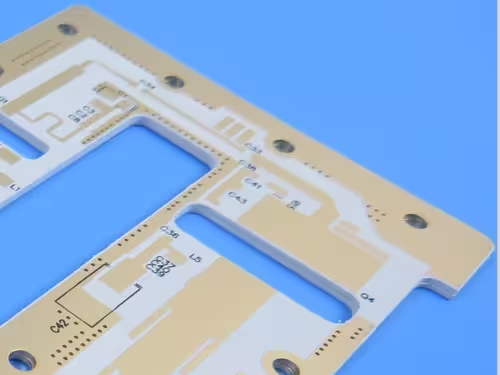
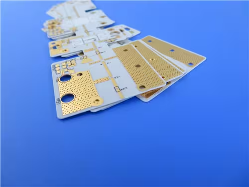
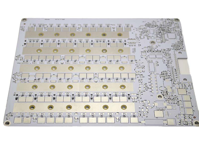
Double-sided PCB Products
Explore our 2-layer PCBs for cost-effective, reliable circuit boards. They are used in consumer electronics, industrial control, and power applications.
-
2-Layer Rogers3035 PCB
Send Inquiry -
2-Layer Rogers 3003 PCB
Send InquiryBase Material: Rogers 3003
Finished Thickness: 0.3mm
Surface Finish: Immersion Gold
-
2 Layer Rogers 4830
Send InquiryBase Material: Rogers 4830
Finished Thickness: 0.2mm
Surface Finish: ENIG
-
2-Layer RF PCB
Send InquiryBase Material: F4BM255
Finished Thickness: 1.6mm
Finish Cu. Weight: 1/1oz
-
2-layer Aluminum PCB
Send InquiryBase Material: Aluminum
Finished Thickness: 1.6mm
Surface Finish: HASL LF
-
2-Layer Custom Legend Color PCB
Send InquiryBase Material: Shengyi S1000-2
Finished Thickness: 1.6mm
Surface Finish: ENIG
Technical Specs
Double-Sided PCB Manufacturing Capabilities
Full fabrication capability range for our double-sided PCB service. All specs subject to DFM review.
| Items | Standard PCB | Advanced PCB | |
|---|---|---|---|
| 1 | Layers Count | 2 layers | |
| 2 | Finished Board Thickness | 16~128 mil (0.4mm – 3.2mm) | / |
| 3 | Max. Panel Size | 24 × 28.5″ (622mm × 723mm) | 24 × 40″ (622mm × 1000mm) |
| 4 | Laminate Materials | FR-4, CEM-3, Mid Tg, High Tg, High CTI, Halogen Free | / |
| 5 | Finished Board Thickness Tolerance | < 1.0mm ±0.10mm (±4mil) 1.0~1.6mm ±0.15mm (±6mil) |
< 1.0mm ±0.075mm (±3mil) 1.0~1.6mm ±0.10mm (±4mil) |
| 6 | Min. Inner Thin Core Thickness | 3mil (0.075mm) | / |
| 7 | Min. Inner Line Width / Spacing | 2.5 / 3.5 mil (0.0635 / 0.089mm) | 2.5 / 2.5 mil (0.0635mm) |
| 8 | Min. Outer Line Width / Spacing | 3.5 / 3.5 mil (0.089 / 0.089mm) | 3.0 / 3.0 mil (0.075 / 0.075mm) |
| 9 | Layer-to-Layer Registration Tolerance | ±3mil (±0.075mm) | / |
| 10 | Copper Foil Thickness | 12μm, 18μm, 35μm, 70μm, 105μm, 140μm (1/3oz – 4oz) | / |
| 11 | Min. Finished Hole Size | 0.2mm | 0.15mm |
| 12 | Min. Drilling Bit Size | 0.2mm | / |
| 13 | Max. Drilling Bit Size | 6.5mm | / |
| 14 | Finished Hole Size Tolerance (PTH) | ±0.075mm (±3mil) | ±0.05mm (±2mil) |
| 15 | Finished Hole Size Tolerance (NPTH) | ±0.05mm (±2mil) | / |
| 16 | Drilling Precision Tolerance (vs CAD data) | ±0.075mm (±3mil) | ±0.05mm (±2mil) |
| 17 | PTH Hole Copper Thickness | 20–30μm | 10–15μm |
| 18 | Max. Aspect Ratio | ≤ 10:1 | 12:1 |
| 19 | Impedance Control | ±10% | ±8% |
| 20 | Min. Solder Mask Opening | 0.05mm (2mil) | 0.02mm (0.8mil) |
| 21 | Min. Solder Dam | 0.076mm (3mil) | 0.063mm (2.5mil) |
| 22 | Surface Finish | OSP, Peelable Solder Mask, Carbon Ink, HASL (lead free), ENIG, I-Ag, I-Tin | OSP, Peelable Solder Mask, Carbon Ink, HASL (lead free), ENIG, I-Ag, I-Tin |
| 23 | OSP Thickness | 0.2–0.5μm | / |
| 24 | V-Cut Angle | 20°, 30°, 45°, 60° | / |
| 25 | Min. V-Cut Co-thickness | 0.25mm | / |
| 26 | Profiling Mode | Routing & Punching | / |
| 27 | Dimensional Tolerance | ±0.10mm (4mil) | / |
| 28 | E-Test Voltage | 250 ± 5V | / |
| 29 | Max. E/T Insulation Resistance | 100 MΩ | / |
| 30 | Min. E/T Conductive Resistance | 20 MΩ | / |
if your design has very limited space or uses high-speed signals, you should consider a 4-layer or multilayer board. Learn the differences between 2-layer and 4-layer PCBs.
Ready to Build Your Double-Sided PCB?
No MOQ — upload your Gerber files and receive a quote in minutes. Prototype quantities ship in 24 hours. ISO 9001 certified factory, global shipping available.
Defibiton
What Is a Double-Sided PCB?
A double-sided PCB (also called a 2-layer PCB) is a printed circuit board with conductive copper traces on both the top and bottom surfaces of the substrate. The two layers are electrically interconnected through plated through-holes (PTH) or vias, enabling more complex circuit routing within a compact board area.
Compared to single-sided boards, double-sided PCB boards offer significantly higher circuit density, reduced electromagnetic interference, and better signal integrity — making them the go-to solution for the vast majority of modern electronic products.
At HXDcircuit, our double-sided PCB manufacturing process uses FR4 as the standard substrate, with High-Tg and specialty laminate options available. Every board goes through our full inspection flow — AOI, flying-probe electrical test, and visual inspection — before shipping.
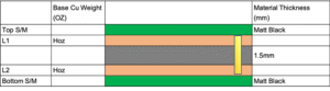
2-Layer PCB Stackup
- Substrate: Provides mechanical support and insulation, typically FR-4.
- Copper Layers: Etching creates circuit traces to transmit electrical signals.
- Solder Mask: Protects copper from oxidation and short circuits; colors include green, blue, red, and black.
- Silkscreen: Prints component identifiers, logos, and test points.
Advantages of Double-Sided PCB
Double-sided PCBs offer the following advantages:
Low Cost
Double-sided PCBs use less material and have a simple manufacturing process. This makes them the most cost-effective choice.They are cost-effective for mass production.
Simple Circuits
If your design has few components and signal lines, a single or double-sided layout is enough without extra internal layers.
Fast Prototype Turnaround
Double-sided PCBs have a simpler manufacturing process with fewer steps, resulting in shorter lead times. For 2-Layer Prototypes,HXD can support you 24–48 hours lead time.
Improved Signal Integrity
Dedicated ground planes and power planes on the second layer reduce EMI and improve overall signal quality.
Wide Material Compatibility
Supports FR4, High-Tg FR4, aluminum, Rogers and flex substrates — adaptable to diverse thermal and electrical requirements.
Real-World References
Double-Sided PCB Stackup Examples
Actual stackup configurations from HXDcircuit production orders — use these as a reference when specifying your 2-layer PCB material and surface finish.
2-Layer PCB Stackup Example 1
| Finished Board Thickness | 1.6+/-10% |
| Application | Consumer Instrument |
| Material | Shengyi S1000-2 |
| Min. Line W/S | 0.1 / 0.1 mm |
| Surface Finish | ENIG |
| Special Features | Different silkscreen colours IPC Class 3 standard No minor scratches on solder mask |
2-Layer PCB Stackup Example 2
| Finished Board Thickness | 1.63+/-10% |
| Application | Medical |
| Material | ISOLA 370HR |
| Min. Line W/S | 0.05/ 0.05 mm |
| Surface Finish | ENIG+Hard Gold Plating on Fingers |
| Special Features | Rigid board to be applied with EMI Shielding Layer |
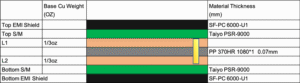
2-Layer PCB Stackup Example 3
| Finished Board Thickness | 1.2+/-10% |
| Application | Communication |
| Type | PTFE PCB |
| Material | Wangling F4BM255 Tg260 |
| Min. Line W/S | 0.2/ 0.2 mm |
| Surface Finish | ENIG |
| Comment | The material lead time for Alon/Teflon is long and the price is very expensive. Wangling is Chinese brand and can use to replace some of the P/N. |
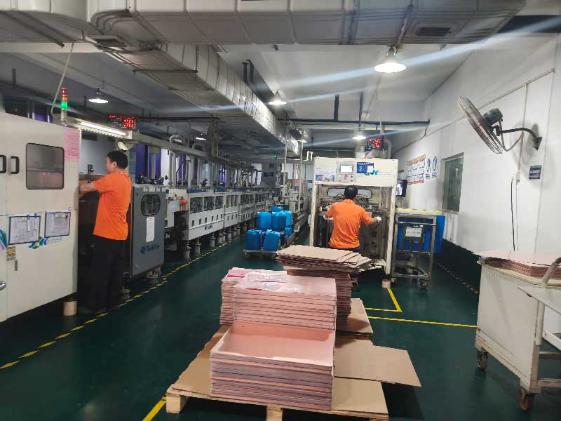
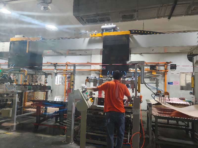
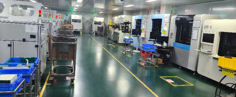
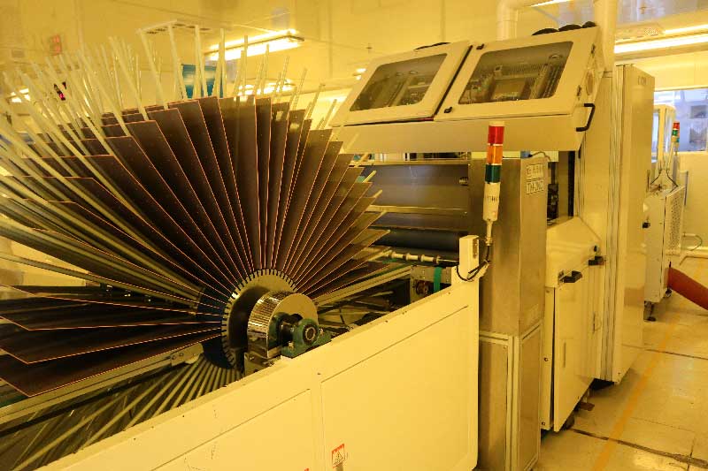
Our Facility
Advanced Equipment for Stable PCB Manufacturing
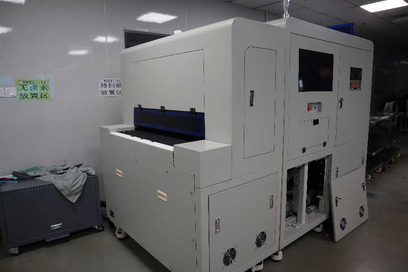
HXD has more than 15 years of experience in 2-layer PCB production. We keep investing in the latest manufacturing and inspection machines. We keep our equipment in great shape, including laser direct imaging and high-precision lamination presses. This ensures your boards are perfect every time.
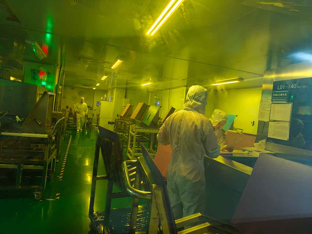
LDI Exposure
Etching
Inner AOI
Innerlayer Laminating
E-test
Automatic Dry Film Laminator
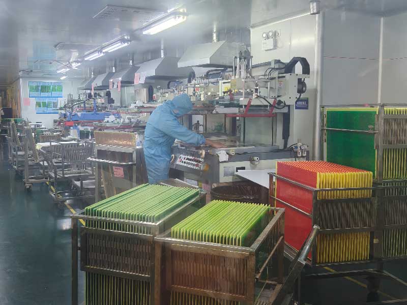
Semi Auto Legend Printing
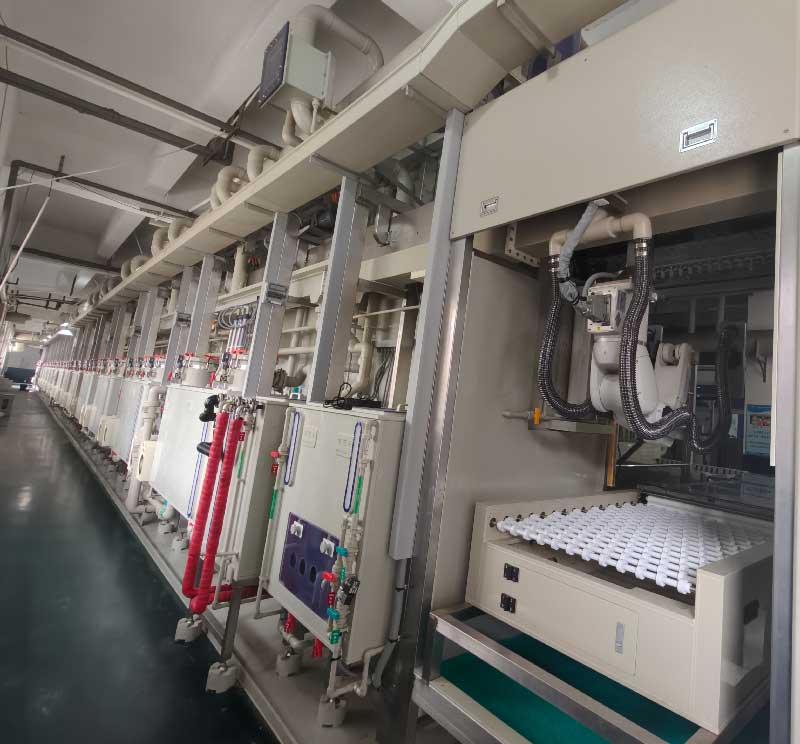
VCP Plating
FAQ
Frequently Asked Questions
Common questions about our double-sided PCB manufacturing service.
What is the difference between single-sided and double-sided PCB?
Is the quality guaranteed for small orders?
When is it Time to Upgrade from Double-sided to 4+ Layer PCB Designs?
High Component Density: When you run out of board real estate and have to add a lot of components to finish the routing with only two layers.
Complex Packaging: With high-performance microprocessors or BGA packages. The pin density of these devices often exceeds what a 2-layer board can route.
High-Speed Signal Needs: Multi-layer boards are preferred for high-frequency or tightly controlled impedance applications since they often provide dedicated power and ground layers.
Do you ship double-sided PCBs internationally?
What file formats do you accept for double-sided PCB orders?
What types of vias are used in double sided PCBs?
What are the design limitations of double sided PCB?
* No dedicated internal power or ground planes
* Limited EMI shielding performance
* Constraints in high-speed signal routing
* Not suitable for high-density BGA designs