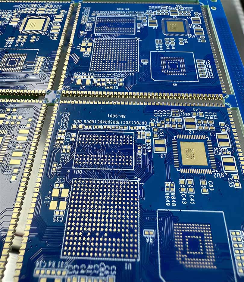
HXD Electronics is located in Guangzhou,founded in 2005, integrating the full production process — lamination, drilling, plating, imaging, surface treatment, and final testing — all completed in-house for total process control.
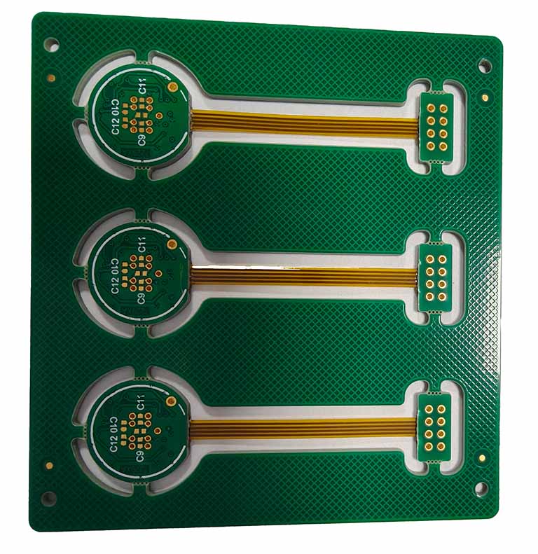
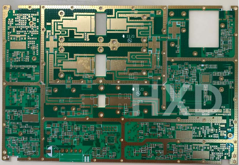
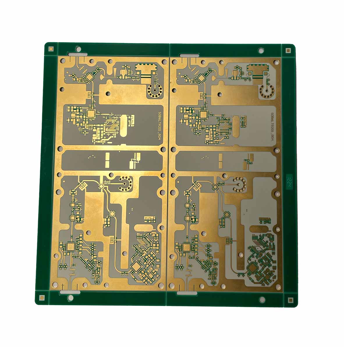
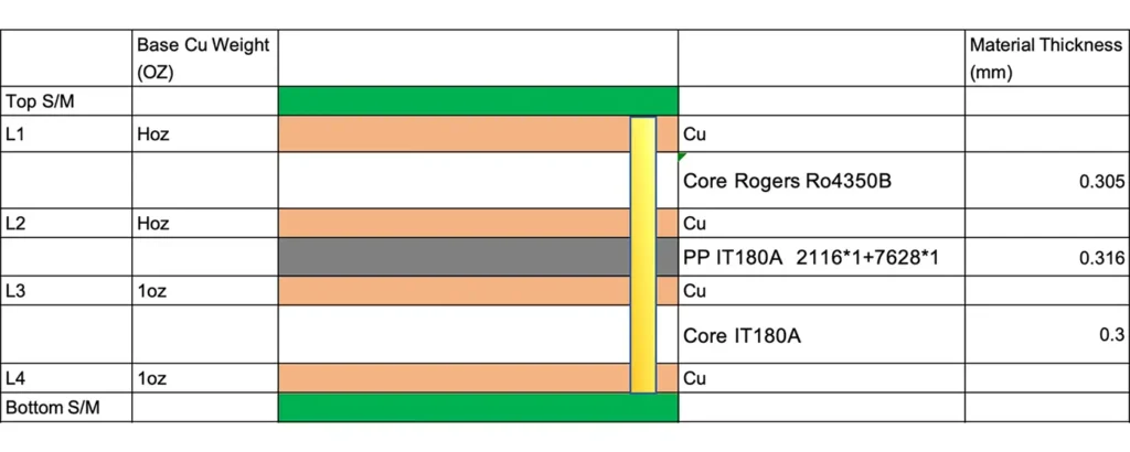
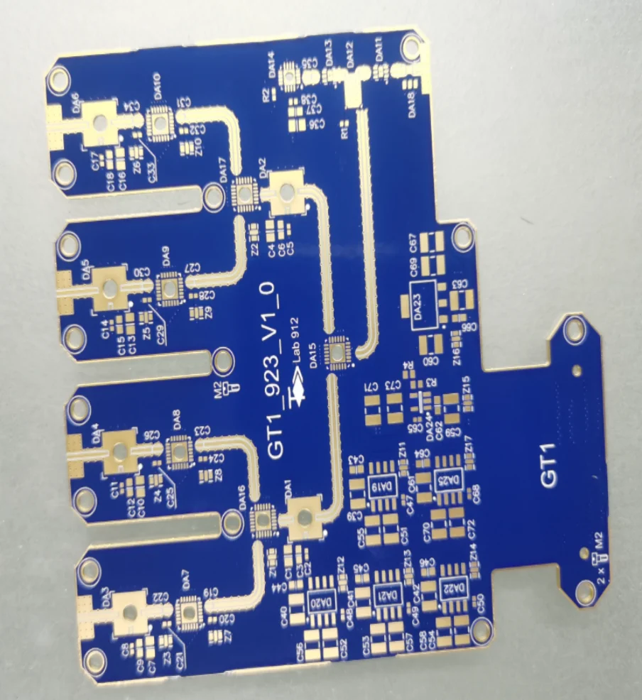
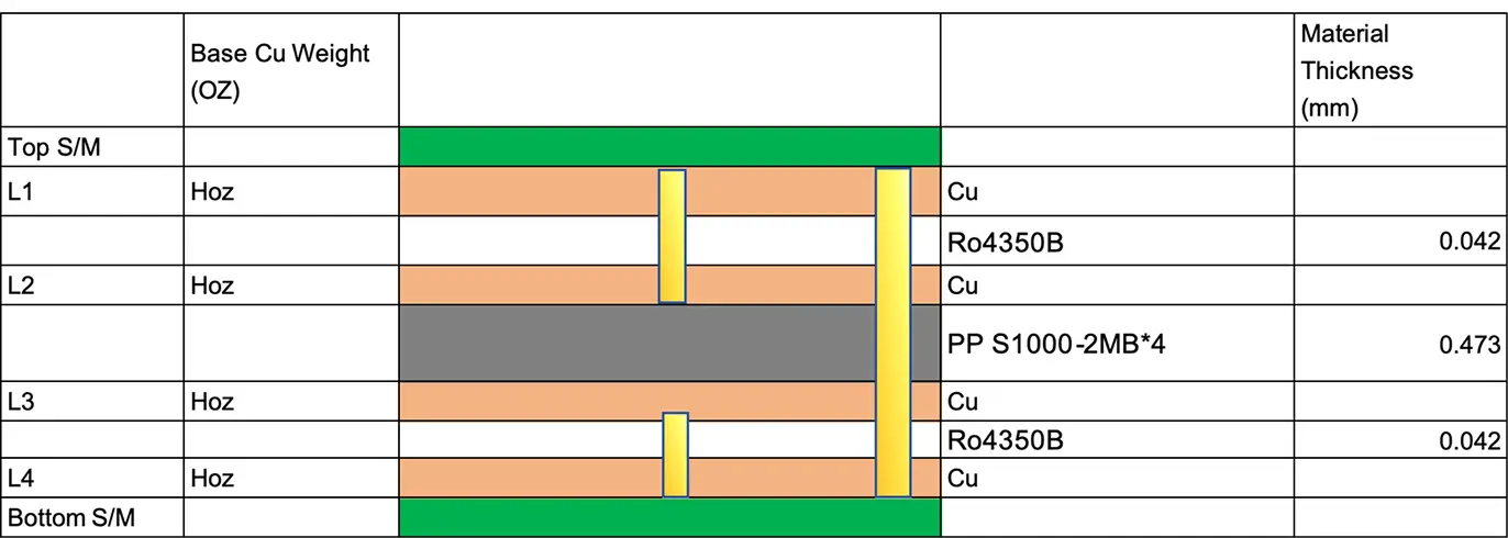
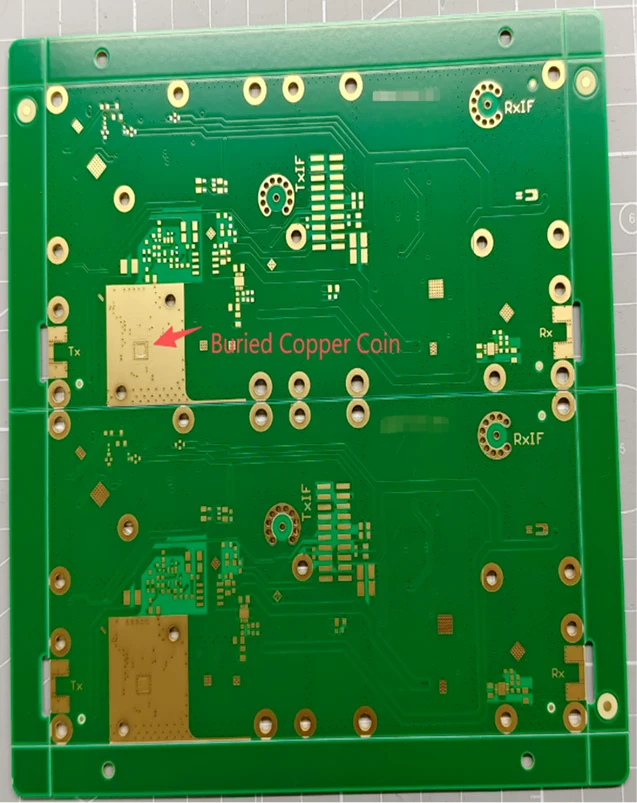
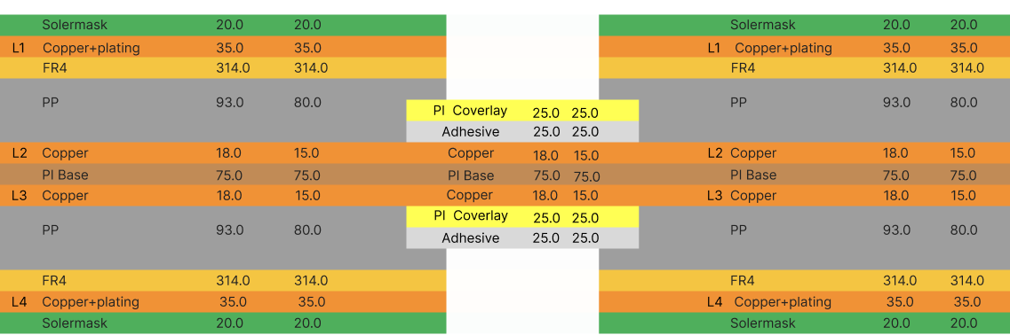
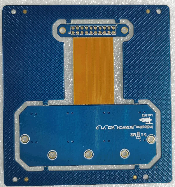
Equipped with advanced automation and precision testing systems, we produce high-quality rigid up to 50layers, rigid-flex and high-frequency, meeting IPC and UL standards.
With professional engineering support, stable supply chain, and efficient workflow, we ensure fast lead times and high reliability for demanding applications in all kinds of industries.