High-Density Design
An 8-layer PCB provides enough layers for micro-electronics, wearable devices, and designs with multiple power islands.
This structure also helps separate different subsystems and improve routing flexibility.
An 8-layer PCB is a multilayer printed circuit board with eight conductive copper layers laminated together. Compared with 4-layer and 6-layer boards, it provides much higher routing density, more reference planes, and better separation between power, ground, and signal layers.
A typical 8-layer design uses multiple signal layers, dedicated ground planes, and dedicated power planes. This makes it easier to control impedance, reduce crosstalk, improve EMI performance, and support dense component layouts.
8-layer PCBs are often chosen for high-speed digital, networking, industrial control, medical, automotive, and communication equipment where electrical performance and board density matter more than minimum fabrication cost.
Typical 8-Layer PCB Stackup

Technical Specs
Comprehensive 8-layer PCB manufacturing capabilities covering stackup design, material selection, copper thickness options, and precision fabrication for diverse applications.
| Items | Standard PCB | Advanced PCB |
|---|---|---|
| Finished Board Thickness | 16~128 mil (0.4mm – 3.2mm) | / |
| Max. Panel Size | 24 × 28.5″ (622mm × 723mm) | 24 × 40″ (622mm × 1000mm) |
| Laminate Materials | FR-4, CEM-3, Mid Tg, High Tg, High CTI, Halogen Free | / |
| Finished Board Thickness Tolerance | < 1.0mm ±0.10mm (±4mil) 1.0~1.6mm ±0.15mm (±6mil) |
< 1.0mm ±0.075mm (±3mil) 1.0~1.6mm ±0.10mm (±4mil) |
| Min. Inner Thin Core Thickness | 3mil (0.075mm) | / |
| Min. Inner Line Width / Spacing | 2.5 / 3.5 mil (0.0635 / 0.089mm) | 2.5 / 2.5 mil (0.0635mm) |
| Min. Outer Line Width / Spacing | 3.5 / 3.5 mil (0.089 / 0.089mm) | 3.0 / 3.0 mil (0.075 / 0.075mm) |
| Layer-to-Layer Registration Tolerance | ±3mil (±0.075mm) | / |
| Copper Foil Thickness | 12μm, 18μm, 35μm, 70μm, 105μm, 140μm (1/3oz – 4oz) | / |
| Min. Finished Hole Size | 0.2mm | 0.15mm |
| Min. Drilling Bit Size | 0.2mm | / |
| Max. Drilling Bit Size | 6.5mm | / |
| Finished Hole Size Tolerance (PTH) | ±0.075mm (±3mil) | ±0.05mm (±2mil) |
| Finished Hole Size Tolerance (NPTH) | ±0.05mm (±2mil) | / |
| Drilling Precision Tolerance (vs CAD data) | ±0.075mm (±3mil) | ±0.05mm (±2mil) |
| PTH Hole Copper Thickness | 20–30μm | 10–15μm |
| Max. Aspect Ratio | ≤ 10:1 | 12:1 |
| Impedance Control | ±10% | ±8% |
| Min. Solder Mask Opening | 0.05mm (2mil) | 0.02mm (0.8mil) |
| Surface Finish | OSP, Peelable Solder Mask, Carbon Ink, HASL (lead free), ENIG, I-Ag, I-Tin | OSP, Peelable Solder Mask, Carbon Ink, HASL (lead free), ENIG, I-Ag, I-Tin |
| V-Cut Angle | 20°, 30°, 45°, 60° | / |
| E-Test Voltage | 250 ± 5V | / |
| Max. E/T Insulation Resistance | 100 MΩ | / |
| Min. E/T Conductive Resistance | 20 MΩ | / |
In addition to 8-layer PCBs, we produce 10-layer PCB, and 12-layer PCB boards.These are ideal for complex and high-performance applications.


We have successfully delivered many complex 8-layer PCB products. Below are some typical 8-layer PCB cases.
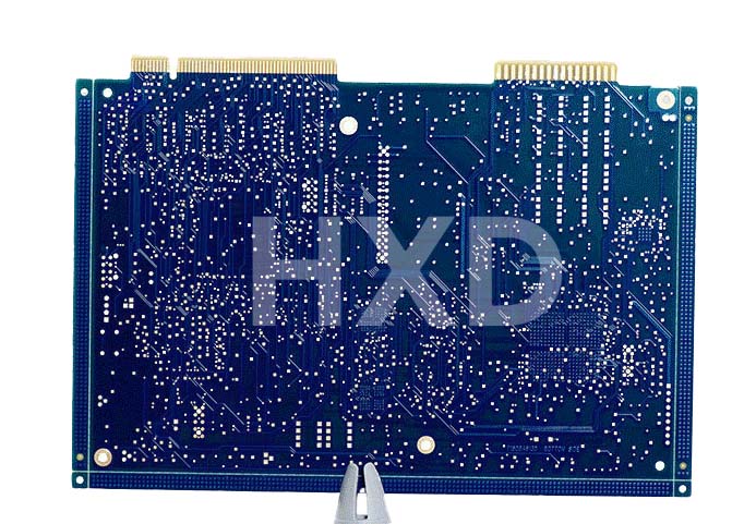
Material: Fr4 Tg170 Board Thickness: 2.0mm Surface Finish: ENIG Certificated: ISO9001 ISO14001 UL
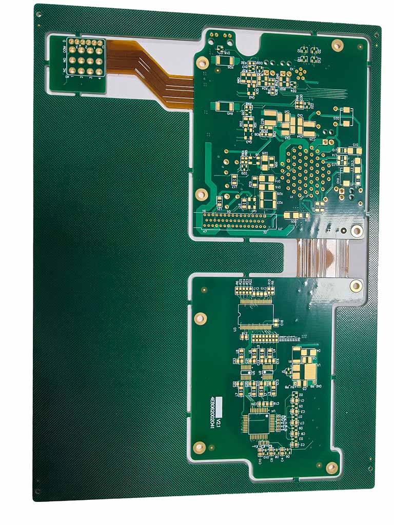
Material: FR4+PI(AP8535R)+Arlon 49N Board Thickness: 1.6mm Surface Finish: ENIG Certificated: ISO9001 ISO14001
Controlled impedance, High-Tg FR4, and Rogers material options available.
Real-World References
Explore real 8-layer PCB stackup examples from HXDcircuit production orders. Use these references to choose the right material, thickness, copper weight, and surface finish for your project.
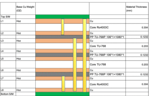
| Finished Board Thickness: | 1.65+/-10%mm |
| Application: | 5G Massive MIMO |
| Layer: | 8L |
| Material: | Ro4003、Tu-768 |
| Surface Finish: | ENIG |
| Certification: | IPC-6012E Class II |
This 8-layer hybrid PCB stackup combines Rogers RO4003C and TU-768 materials. Rogers layers support high-frequency signal performance, while FR-4 inner layers help reduce cost. With blind vias and multilayer routing, this structure is suitable for RF, 5G, radar, and compact high-speed designs. View Product Images.
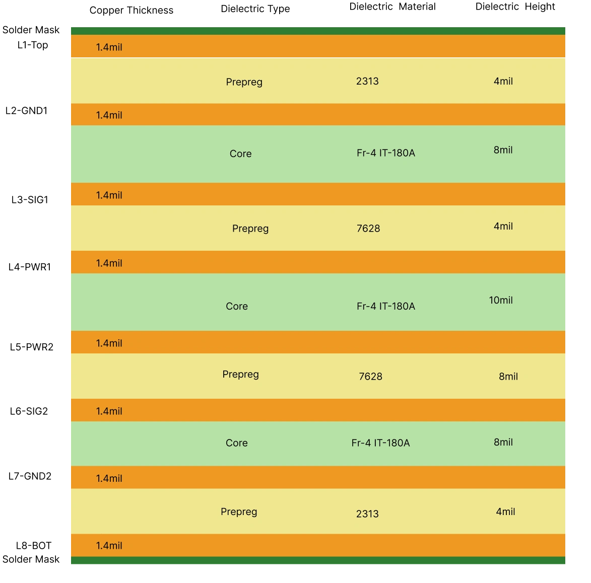
| Finished Board Thickness: | 1.6+/-10%mm |
| Layer: | 8L |
| Laminate: | FR4 |
| Laminate brand: |
[ITEQ, IT-180 A (TG180)] or [Shenyang, TG170 FR4] |
| Surface Finish: | Immersion Gold |
| Certification: | IPC-6012E Class II |
This 8-layer PCB stackup uses IT-180A high-Tg FR-4 material and 1 oz copper on each layer. The 4 mil dielectric spacing between L1-L2 and L8-L7 supports stable impedance control for 50Ω single-ended and 100Ω differential traces. With multiple reference planes, this structure is suitable for high-density routing, industrial control boards, and high-speed electronic products. View Product Images.
HXD has rich experience in 8-layer PCB design and production. For more stackup references, you can view more rigid-flex PCB stackup examples or read our 8-layer PCB design guide.
Designers often choose 8-layer PCBs for high-speed signals, stable power delivery, and better EMI shielding. They use them in the following applications:
An 8-layer PCB provides enough layers for micro-electronics, wearable devices, and designs with multiple power islands.
This structure also helps separate different subsystems and improve routing flexibility.
An 8-layer’s stackup is symmetrical. This structure effectively controls impedance accuracy and supports the stable transmission of high-speed signals above 28Gbps.
In addition, the design usually places signal layers next to ground or power planes. This can reduce crosstalk between signals by over 30% and provide a clear return path.
An 8-layer PCB can reduce electromagnetic interference (EMI) because it has more space for ground and power planes.
These planes give signals a shorter return path and help shield signal layers from noise. This reduces radiation, lowers noise coupling, and improves signal stability.
An 8-layer PCB provides better thermal management. It has more internal copper layers and larger heat-spreading paths.
Ground and power planes help spread heat across the board. Thermal vias move heat away from hot components to inner layers or heat sinks.
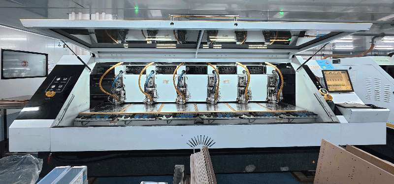
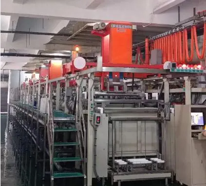
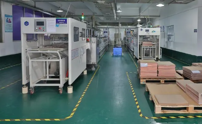
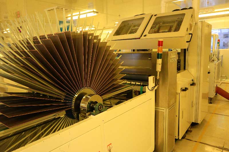
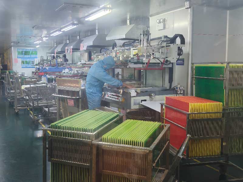
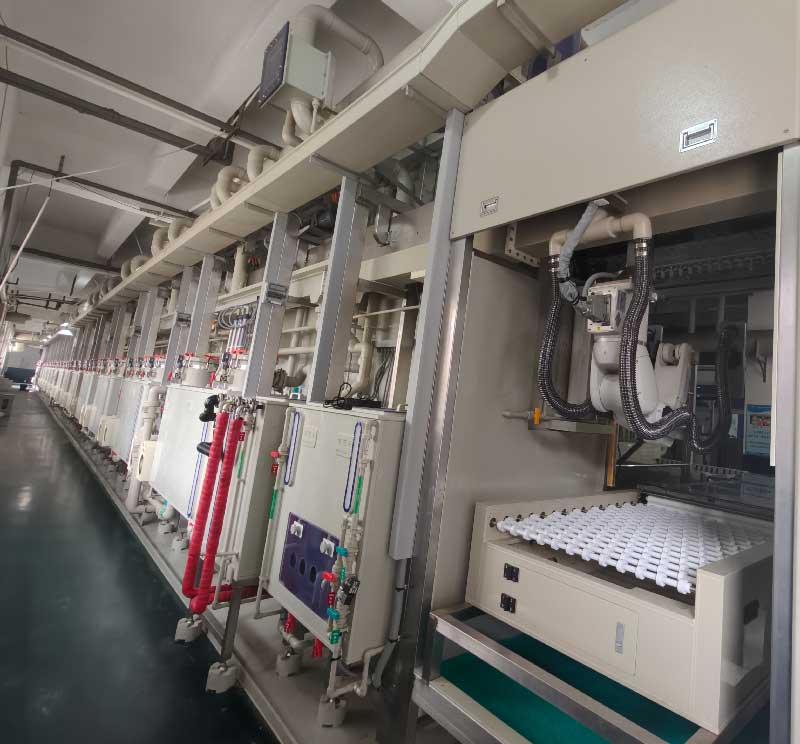
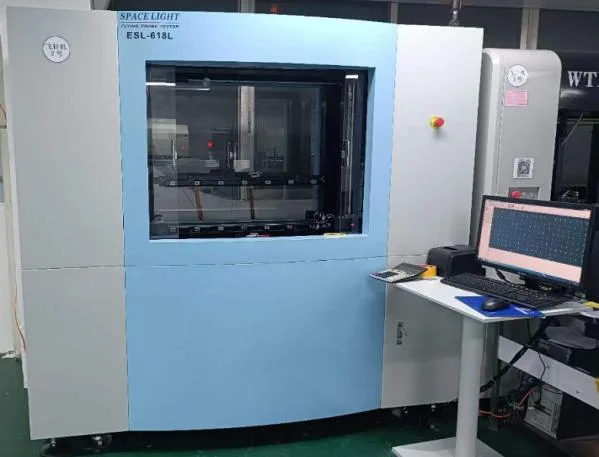
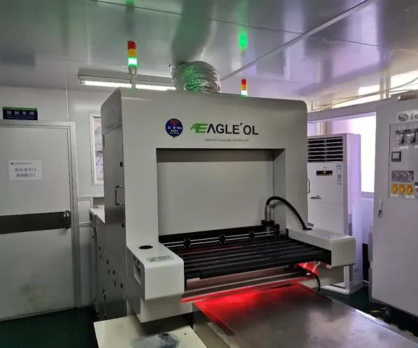
Our Facility
HXD has more than 15 years of experience in multilayer PCB production. We keep investing in the latest manufacturing and inspection machines. We keep our equipment in great shape, including laser direct imaging and high-precision lamination presses. This ensures your boards are perfect every time.
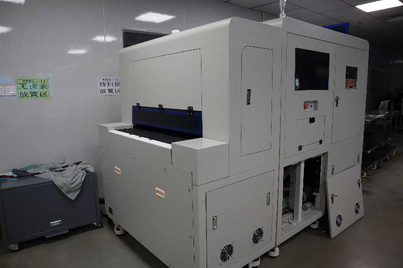
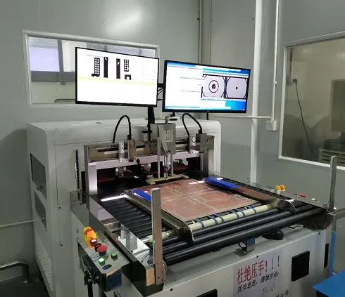
Quality Assurance
We manufacture every 8-layer PCB through a structured quality process. This ranges from inner layer inspection to final board verification, ensuring your boards perform exactly as designed.
Every board is fully tested for open circuits, short circuits, and net continuity before shipment. We use flying probe or fixture-based testing depending on volume, ensuring zero electrical defects reach your assembly line.
High-resolution AOI systems scan the inner and outer layers. They find trace defects, missing pads, solder mask misalignment, and other visual issues. This helps catch problems early, saving money.
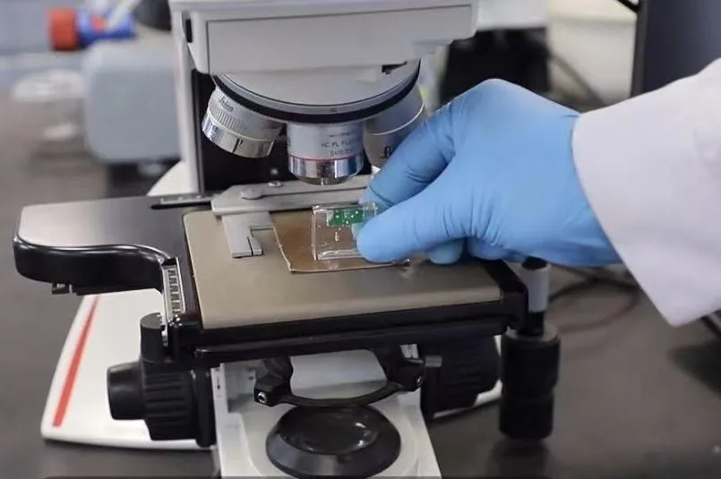
We use micro-sectioning to check the inside of the PCB. By cutting a small sample and viewing it under a microscope, we can inspect via plating, layer alignment, and bonding quality. This helps make sure every board is strong and reliable.

Before packaging, each board gets a detailed final inspection. We check dimensions, surface finish, hole quality, silkscreen accuracy, and overall workmanship. This all meets IPC Class 2 or Class 3 standards.
All quality records are traceable and available upon request. We stand behind every board we ship.
8-layer PCBs work well for compact electronic systems, high-speed circuits, and designs that cannot be easily routed on 2-layer or 4-layer boards.

Telecommunications equipment often uses 8-layer PCBs for high-speed data transmission, RF modules, routers, switches, and base station systems.
Multiple ground and power planes help improve signal stability, reduce EMI, and support controlled routing for complex communication circuits.
Industrial control systems use 8-layer PCBs in PLCs, motor drives, automation controllers, and power control modules.
The multilayer structure improves noise resistance. It supports stable power distribution, and helps the board work well in harsh electrical environments.
Consumer electronics often need compact PCB designs with many components and complex routing. 8-layer PCBs provide enough space for dense circuits, multiple power zones, and high-speed interfaces.
They are suitable for smart devices, wearables, tablets, and home electronics.
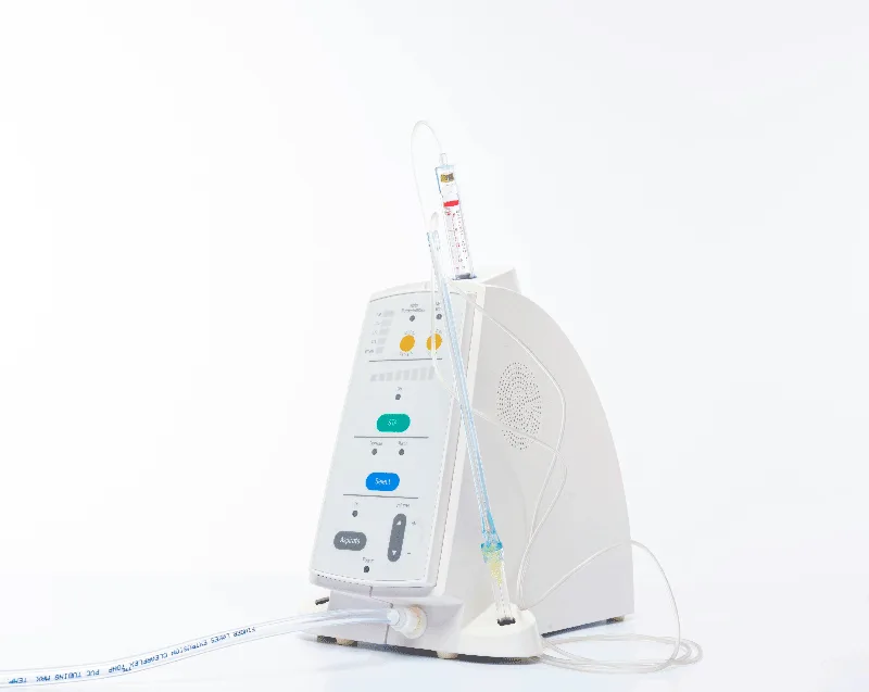
Medical electronic devices need stable signals, low noise, and reliable performance. 8-layer PCBs help separate sensitive analog circuits from digital circuits.
People often use them in monitoring devices, portable medical equipment, imaging systems, and wearable health products.
Upload your design files and get engineering feedback, stackup support, and a fast quote for prototype or production.
FAQ