The Ultimate 8-Layer PCB Stackup Guide for High-Speed Design
Think Deeper with AI:
Introduction
A well-designed 8-layer PCB stackup can improve impedance control, reduce EMI, and support better signal integrity. This makes it suitable for complex and high-speed electronic systems.
In this guide, we will show you how to optimize your 8-layer stackup. Learn how to build more stable and reliable multi-layer PCB solutions for your next project.
Why Stackup Design is Critical for High-Speed Circuits
Stackup design is critical for high-speed circuits because it controls how signals, power, and return currents move through the PCB. When signal frequency reaches hundreds of MHz or even GHz, the PCB is no longer just a carrier for components. It becomes part of the signal path.
A good stackup keep impedance stable. High-speed signals often need 50Ω single-ended or 100Ω differential impedance. To reach these targets, designers must control trace width, copper thickness, dielectric thickness, and material Dk.
Stackup design also affects the return path. High-speed current usually returns through the reference plane under the signal trace. When the signal layer stays close to a solid ground or power plane, the return path becomes shorter and more stable. This helps reduce EMI, loop inductance, and signal distortion.
A poor stackup can cause reflection, crosstalk, power noise, and data errors. For this reason, designers should review the stackup structure early in the PCB design process.
They should also check material selection, core and prepreg thickness, and impedance targets.
Typical 8-Layer PCB Stackup Configuration
Choosing the right PCB stackup is the foundation of a successful 8-layer PCB design. A well-planned stackup helps control impedance, reduce EMI, and ensure reliable high-speed signal transmission.
You can use our PCB Stackup Design Tool to start your 8-layer PCB planning faster. We have built in many common 8-layer stackup templates, including high-speed, power-enhanced, and traditional symmetric structures. These templates help you compare different stackup options before manufacturing.
To help you balance performance and cost, we summarize proven structures used in the industry. Below are three recommended 8-layer PCB stackup configurations for different application needs.
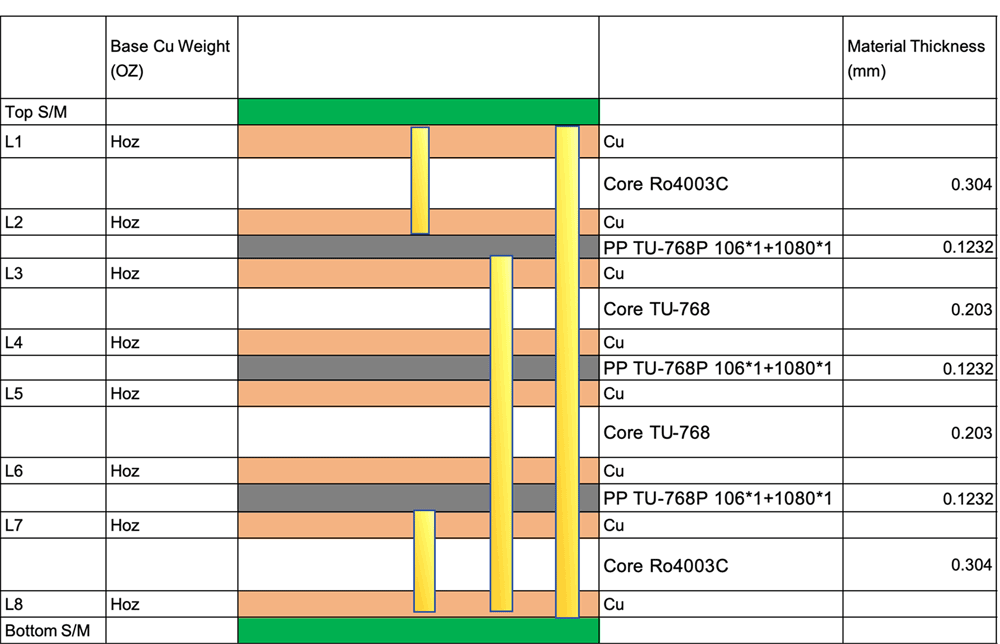
Example1: Standard High-Performance Stackup
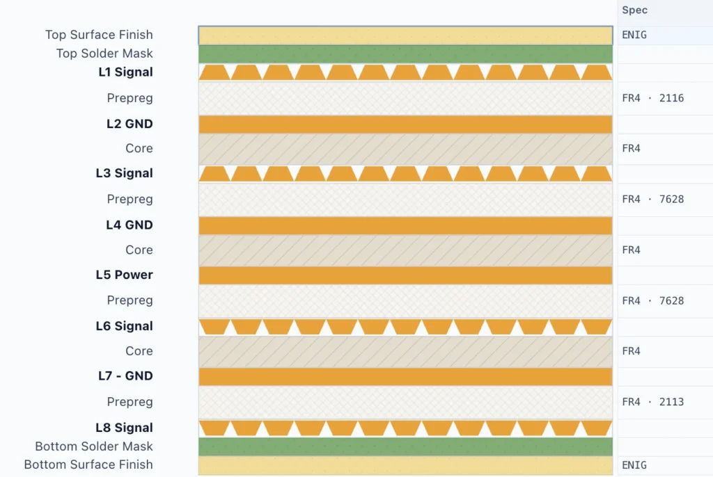
This is one of the most widely used 8-layer stackup configurations in the PCB industry. Its main advantage is strong EMI shielding. Two ground planes create a stripline structure and enclose the inner signal layers, L3 Signals and L6 Signals. This design provides a short return path and works well for high-density, high-speed PCB designs.
Example2: Power-Enhanced Type
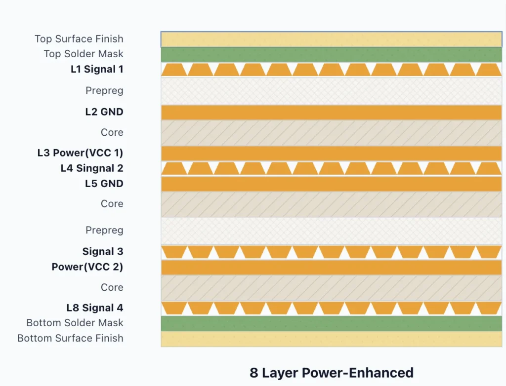
This 8-layer PCB stackup is a power-enhanced structure for designs that need both routing space and stable power delivery. It includes four signal layers, two ground planes, and two power planes. The nearby ground plane under the top signal layer helps provide a stable return path and supports impedance control. The power and ground layers also improve the power distribution network and help reduce power noise.
This stackup works well for FPGA boards and embedded control boards. It is also suitable for industrial electronics, servers, and digital systems with multiple power rails.
However, for very high-speed signals, you should check the reference planes and avoid routing over split power areas.
Example3: Low-Cost / Traditional Symmetric Type
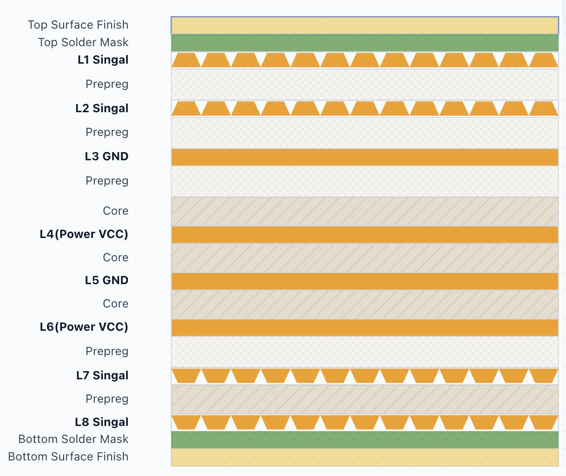
This traditional symmetric 8-layer PCB stackup is suitable for general digital designs, cost-sensitive products, and mass production. Its main advantage is good stackup balance. The signal layers are placed on both sides, while the power and ground planes are arranged near the center.
This structure helps reduce board warpage during lamination and reflow soldering. This is important for stable SMT assembly and good production yield. It also uses a standard multilayer process, making it easier to control cost in volume production. The power and ground planes also support a more stable power distribution network.
However, this stackup is not the best choice for very high-speed signals. The top and bottom signal layers do not have nearby ground reference planes. This may reduce EMI shielding and make impedance control more difficult.
These 8-layer PCB stackups are common structures used in HXD production projects. If your project needs a custom 8-layer stackup, use our PCB stackup design tool. You can customize 8-layer stackup options to match your design needs.
Contact Us for engineering support and manufacturing review.
How to Master Impedance Control in 8-Layer PCB Design
When designing an 8-layer PCB, impedance control mainly depends on the stackup structure, material parameters, and trace geometry. To calculate impedance correctly, you need to control several key variables:
- Dielectric thickness (H): the distance between the signal layer and the reference plane. A smaller distance results in lower impedance.
- Trace width (W): Wider traces have lower impedance.You can use our online tool to calculate the right trace width.
- Copper thickness (T): common values are 0.5 oz or 1 oz. Learn more about copper thickness.
- Dielectric constant (εr): determined by the base material. For example, FR-4 typically has an εr of about 4.2–4.5.
- Differential spacing (S): for differential pairs. Smaller spacing increases coupling and reduces differential impedance.
The dielectric thickness between the signal layer and the reference plane is the most critical parameter for impedance control. A larger thickness leads to higher impedance. For this reason, PCB manufacturers usually provide a stackup parameter table during the design stage. This helps ensure accurate impedance matching.
During routing, the following design rules are also important:
- Impedance traces should not cross a split in the reference plane (split plane). This can cause impedance discontinuity and affect signal integrity.
- Each via can affect impedance because it adds parasitic capacitance and inductance. If the signal needs to change layers, place a ground via near the signal via to support a stable return path.
After manufacturing, the PCB supplier often performs TDR (Time Domain Reflectometry) testing.
Key Design Rules for 8-Layer High-Speed PCBs
To ensure stable performance of high-speed signals, the following design rules should be followed.
1. The 20H Rule
20H is a PCB design rule used to reduce edge radiation and EMI. “H” means the dielectric thickness between the power plane and ground plane. The design pulls the power plane back from the ground plane edge by 20 × H. This helps the ground plane shield the power plane edge.
2. Strict Stackup Symmetry
Your PCB stackup must be perfectly symmetrical from the center line. This includes copper weight, dielectric thickness, and material types. Symmetry prevents the board from warping during high-temperature reflow soldering, ensuring high SMT production yields.
3. Via Management & Layer Changes
When high-speed signals change layers, the impedance can become less stable.
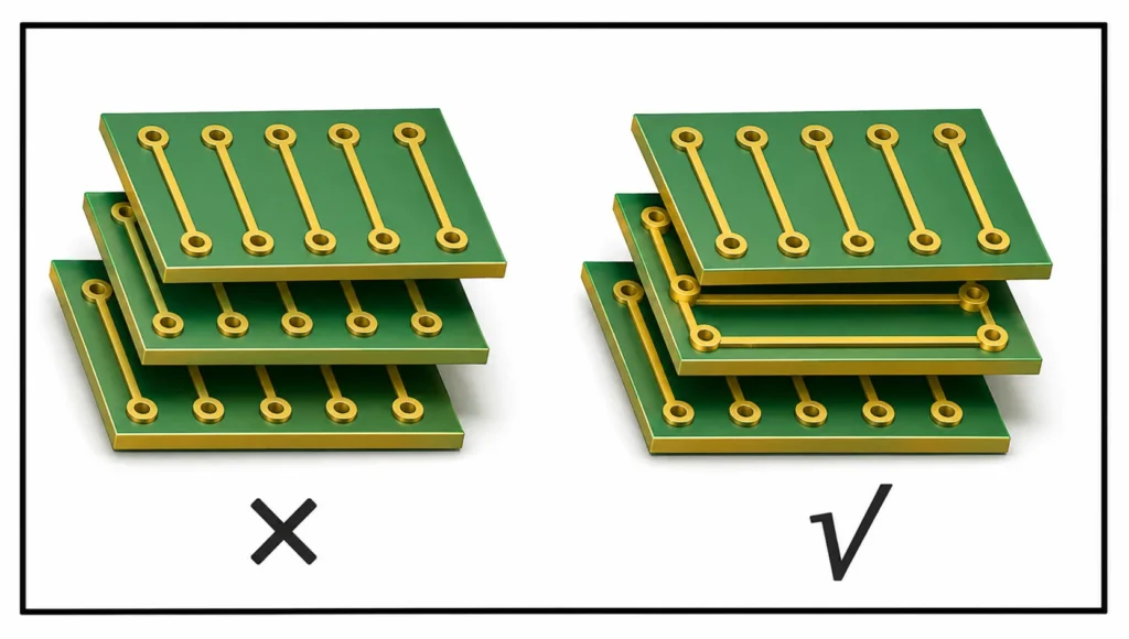
When a signal moves from the Top layer to the Bottom layer, place a ground via close to the signal via. This provides a continuous return current path and reduces via inductance.
For very high-speed signals above 10 Gbps, use back drilling to remove unused via stubs. This helps reduce signal reflection and improves signal integrity.
4. Orthogonal Routing
Route adjacent signal layers in different directions. For example, Layer 3 can use horizontal routing, while Layer 4 uses vertical routing. This reduces trace overlap and helps control broadside crosstalk. This is also called X-Y routing.
5. Continuous Reference Planes
High-speed traces must always have a solid, unbroken reference plane directly underneath. Never route a high-speed signal across a split in the power or ground plane.
Avoid routing high-speed signals across split planes. A split plane makes the return current take a longer path. This can reduce signal quality and increase interference.
Material Selection for 8-Layer PCB
In 8-layer PCB design, material selection is not only about cost. As the layer count increases, the electrical performance and thermal stability of the PCB become more important.
Based on different application needs, materials for 8-layer PCBs can be divided into three categories:
| Type | Materials | Key Features | Applications |
|---|---|---|---|
| Standard Industrial | Isola 370HR IT-180A S1000-2M | High Tg (170°C–180°C), excellent thermal stability, compatible with lead-free soldering. | Industrial control, medical devices, and most standard high-speed PCBs (< 3GHz). |
| Mid-to-Low Loss | Panasonic Megtron 4/6 Isola TerraGreen Nelco N4000-13 | Low Df and stable Dk, suitable for high-speed serial signals. | Servers, storage networking, and telecom equipment (5Gbps – 20Gbps). |
| High Frequency / RF | Rogers 4350B Rogers 4003C | Excellent high-frequency performance and very low moisture absorption. Often used on the outer layers in hybrid stackups. | Radar systems, satellite communication, and 5G RF modules. |
To balance performance and cost, we often recommend a hybrid stackup. Use Rogers material on the top and bottom layers for high-speed signals. Use lower-cost FR-4 for the inner power and ground layers.
This design keeps critical signals stable and can reduce total manufacturing cost by about 30%–50%.
Manufacturing Challenges
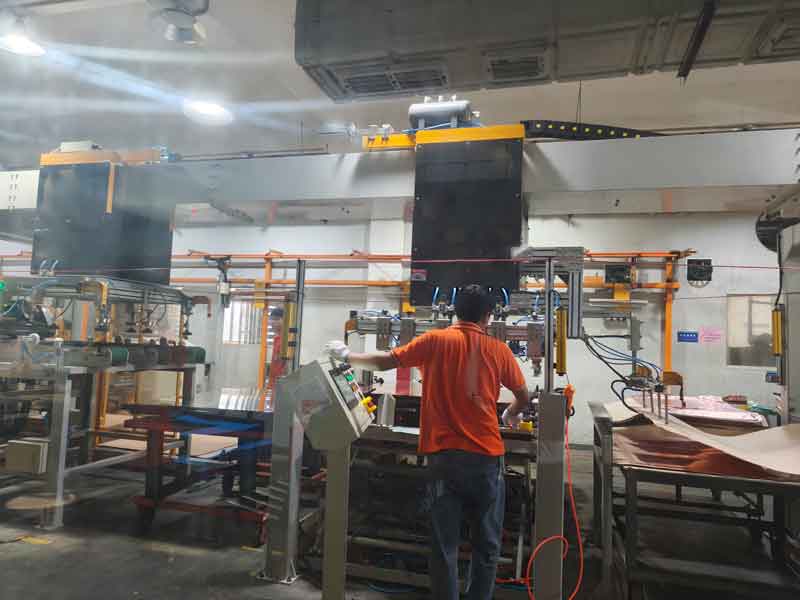
8-layer PCB manufacturing is more complex than producing basic 4-layer or 6-layer boards. As the layer count increases, stable lamination, precise drilling, and reliable quality control become more important.
1. Inner Layer Registration
During lamination, all 8 layers of copper and prepreg must align perfectly. Even a microscopic shift can cause the drill to miss the copper pad (Annular Ring), leading to short or open circuits.

HXD Circuit uses LDI and CCD alignment systems to improve layer alignment before lamination. This helps reduce layer shift and supports reliable multilayer PCB production.
2. Complex Lamination
An 8-layer board requires high heat and pressure to bond multiple materials together. If the stackup is asymmetrical or the pressure is uneven, the board will warp, making SMT assembly impossible. Poor cleaning or trapped air can also cause internal bubbles, leading to delamination later.
3. High Aspect Ratio Drilling
An 8-layer board is usually 1.6mm or thicker. As the board gets thicker and holes get smaller, the “Aspect Ratio” (thickness vs. hole diameter) increases.
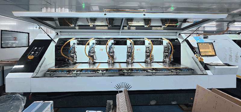
This makes drills prone to breaking and makes it hard for plating solution to reach the center of the hole. Precise speed control and high-penetration plating are essential for uniform copper walls.
4. Sequential Lamination for Blind & Buried Vias
Many 8-layer designs use blind or buried vias to save space. This requires the board to go through the lamination and drilling process multiple times. Every extra cycle increases the cost and the risk of yield loss.
5. Tight Impedance Tolerance
8-layer boards often carry high-speed signals like PCIe 4.0/5.0. Small changes in dielectric thickness or trace width will ruin the impedance. Manufacturers must have expert control over the Etch Factor and perform TDR (Time Domain Reflectometry) testing before shipping.
6. Inner Layer Adhesion
8-layer PCBs usually include large-area power and ground planes. To improve resin bonding, we use brown oxide or black oxide treatment to roughen the copper surface before lamination. This helps reduce the risk of delamination during soldering.
Conclusion
An 8-layer PCB stackup is only one part of a successful design. You also need to consider material selection, impedance control, precise layer alignment, and manufacturing quality. These factors help improve signal performance, and production yield.
If your project needs custom 8-layer PCB fabrication, HXD Circuit can support you from stackup review to stable production. You can order 8-layer PCB or visit our 8-layer PCB manufacturing service page to review our capabilities, and engineering support.
Need a Reliable 8-Layer PCB Stackup?
FAQS
How much more does an 8-layer PCB cost compared to 4 or 6-layer boards?
An 8-layer PCB usually costs about 20%–40% more than a 6-layer board, and even more compared to a 4-layer board. The cost increase mainly comes from:
-
Material usage: More copper, cores, and prepregs are required.
-
Process complexity: Longer lamination cycles, stricter layer alignment, and more drilling time.
-
Yield control: More layers make the board more sensitive to defects (like inner layer misalignment), increasing manufacturing difficulty.
What are some cost-saving tips for 8-layer PCB design?
You can optimize costs with the following methods:
-
Optimize panelization: Design the board size to maximize use of standard production panels (e.g., 18” x 24”).
-
Avoid over-design: Use through-hole vias instead of blind or buried vias unless routing is very dense.
-
Keep standard trace width: Maintain trace/space above 4 mil. While 3 mil is possible, tighter specs reduce yield and increase cost.
-
Surface finish selection: For non-high-speed or non-precision slots, OSP or standard ENIG is more cost-effective than thick gold or ENEPIG finishes.
What are the key factors affecting 8-layer PCB cost?
-
Base Material Selection – Standard FR-4 is cheaper. High TG materials (TG170, TG180) or low-loss materials (Rogers, Isola) for high-speed signals significantly increase cost.
-
Stackup & Board Thickness – The standard 1.6mm thickness is most economical. Special stackups, ultra-thin boards, or heavy copper increase cost due to more complex lamination.
-
Via Technology – Through-hole vias are the cheapest. Blind or buried vias require multiple drilling and lamination cycles, raising the cost.
-
Controlled Impedance – Strict impedance tolerance (e.g., ±5% or ±10%) for single-ended or differential signals requires extra impedance testing and process adjustments, adding technical service fees.
-
Surface Finish – HASL is cheapest, while ENIG or Hard Gold costs more but offers better flatness and solder reliability, making them common for 8-layer PCBs.
When should you upgrade from a 6-layer to an 8-layer PCB?
Consider upgrading to an 8-layer PCB in the following cases:
-
High signal integrity requirements: When trace density is high and a 6-layer board cannot provide complete reference planes for all critical signals.
-
High-speed interfaces: For DDR4/DDR5, PCIe Gen 4/5, or 10G+ Ethernet, finer impedance control is needed.
-
Strict EMC/EMI standards: 8 layers provide more shielding layers to reduce electromagnetic radiation and help pass certifications.
-
Complex power architecture: When the system has multiple voltage rails, extra power planes are needed to maintain power integrity (PI).