PCB Via Types Explained: Through-Hole, Blind, Buried, Microvia, and Via-in-Pad
PCB vias are small plated holes that connect different copper layers in a printed circuit board. They may look simple, but they can affect PCB routing space, signal quality, and manufacturing cost.
This guide explains the main pcb vias types in simple terms. You will learn how to choose the right via type for your PCB project.
Why PCB Vias Matter in PCB Design
PCB vias affect routing, signal quality, cost, and board reliability.
They help designers:
- Connect different PCB layers
- Save routing space
- Move signals between layers
- Carry power and current
- Create thermal paths
- Improve layout flexibility
But vias also add manufacturing limits. Small vias, blind vias, buried vias, and microvias need better process control. They may also increase PCB fabrication cost.
Main PCB Via Types
PCB designers can choose from several via types based on routing needs, board density, and manufacturing limits. Each type connects PCB layers in a different way and fits different design needs.
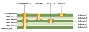
The table below lists common via types used in the PCB industry:
| Via Type | Layers Connected | Common Use | Cost Level |
|---|---|---|---|
| Plated through-hole vias | Top layer to bottom layer | Standard PCB fabrication | Low |
| Blind vias | Outer layer to inner layer | HDI PCB, BGA routing | Medium to high |
| Buried vias | Inner layer to inner layer | Dense multilayer PCB | High |
| Microvias | Usually nearby layers | HDI PCB, fine-pitch BGA | High |
| PCB via in pad | Via inside component pad | BGA, compact PCB layout | High |
Plated Through-Hole Vias
Plated through-hole vias are the most common via type in PCB manufacturing. They pass from the top layer to the bottom layer of the board and create an electrical connection between layers.
PCB manufacturers often choose plated through-hole vias for standard PCB builds because they are simple, reliable, and low-cost.
PCB manufacturers make them by drilling holes, cleaning the hole walls, adding a thin copper layer, and then electroplating more copper inside the holes.
These vias are reliable, low-cost, and easy to inspect. They work well for standard 2-layer, 4-layer, and many multilayer PCB designs.
Advantages of Plated Through-Hole Vias
Plated through-hole vias offer several benefits:
- Low cost — Helps reduce PCB fabrication cost for standard board designs.
- Easy to manufacture — Uses a common PCB process that most manufacturers can support.
- Strong reliability — Provides stable layer-to-layer connection for many PCB applications.
- Easy to inspect and test — Makes quality checks easier during PCB manufacturing and final inspection.
- Good for many industrial products — Fits a wide range of electronic products, control boards, and power circuits.
They are also accepted by almost all PCB manufacturers. This makes them a safe choice for many projects
Limitations of Plated Through-Hole Vias
Plated through-hole vias also have some limits:
- They use space on every PCB layer.
- They are not ideal for high-density PCB designs.
- They may create via stubs in high-speed PCB designs.
- They can make routing harder in fine-pitch BGA areas.
In high-speed PCB layouts, unused via sections may create via stubs and affect signal quality. For compact HDI boards or fine-pitch BGA routing, blind vias or microvias may be a better choice.
Blind Via PCB
In a blind via PCB, blind vias connect an outer layer to one or more inner layers without extending through the whole board.The image shows an example of blind vias in HXD’s 8-layer PCB.
Blind vias are useful in HDI PCB designs, BGA routing, and dense layouts. They save space because they do not pass through every layer.
Blind vias usually cost more than plated through-hole vias. They need more process control and may need laser drilling or controlled depth drilling.
When to Use Blind Vias
Blind vias are useful when the design has:
- Dense component layout
- Fine-pitch BGA
- Limited routing space
- HDI PCB fabrication
- Need for shorter layer-to-layer connections
- Compact product size
They can help designers escape signals from dense components. This is common in smartphones, medical devices, communication modules, and compact electronics.
Blind Via Manufacturing Considerations
Blind vias are more complex than standard through-hole vias.
Key points to check include:
- Blind vias may need laser drilling.
- Some designs may need controlled depth drilling.
- The process needs stronger control.
- You may need extra lamination steps.
- Cost and lead time may increase.
Designers should discuss blind via PCB requirements with the PCB manufacturer early. This helps avoid redesign, cost surprises, and production delays.
Buried Via PCB
A buried via PCB uses vias that connect inner layers only. You cannot see these vias from the outside the board.
For example, a buried via may connect layer 2 to layer 9 in a 10-layer PCB.
Dense multilayer PCB designs use buried vias. They help save outer layer space for components and routing. This can be useful when the board has many signals and limited area.
Advantages of Buried Vias
Buried vias can help with advanced PCB layouts.
Main benefits include:
- Save outer layer routing space
- Help dense multilayer routing
- Useful for complex PCB stackups
- Support advanced signal routing
- Reduce routing blockage on top and bottom layers
They are helpful when standard vias cannot provide enough routing freedom.
Limitations of Buried Vias
Buried vias also bring extra challenges:
- Higher manufacturing cost
- More lamination steps
- Longer lead time
- Harder inspection and quality control
- More stackup planning needed
Buried vias increase manufacturing cost and production time because they require a more complex fabrication process.
The PCB supplier should review the stackup before production.
Microvia PCB

A microvia PCB uses tiny vias, often made by laser drilling. Designers usually use microvias to connect nearby layers, such as layer 1 to layer 2.
Microvias are common in HDI PCB and fine-pitch BGA designs. They help improve routing density and reduce board size.
Compared with standard vias, microvias are smaller and need more advanced manufacturing. They are useful, but you should not use them without reason. Too many advanced via structures can increase cost and reliability risk.
Stacked Microvia
A stacked microvia means multiple microvias are placed vertically on top of each other. This structure saves space and allows highly dense routing.
Stacked microvias are useful in advanced HDI boards. But they are harder to manufacture. They also need careful reliability review.
Possible concerns include:
- Lamination stress
- Copper plating quality
- Thermal cycling reliability
- Higher production cost
Use stacked microvias only when the layout truly needs them.
Staggered Microvia
A staggered microvia structure places each microvia offset from the next layer connection instead of stacking them vertically.
This structure usually needs a little more space than stacked microvias. But it is often easier to manufacture and may offer better reliability.
For many HDI designs, staggered microvias can be a better balance between routing space and manufacturing risk.
Microvia Design Tips
Before using microvias, check these points:
- Confirm minimum microvia size with the manufacturer.
- Avoid unnecessary stacked microvias.
- Check the aspect ratio.
- Review reliability for high-stress products.
- Confirm laser drilling capability.
- Check the HDI stackup early.
Plan a microvia PCB with the PCB manufacturer before the final layout.
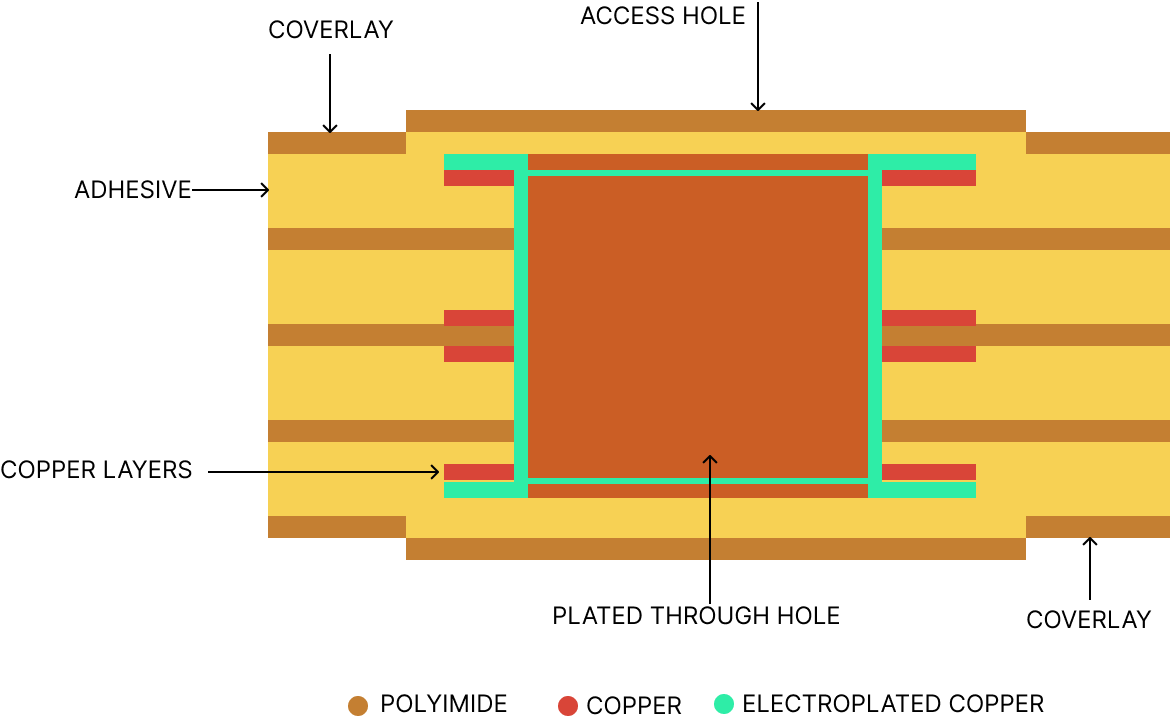
PCB Via in Pad
In PCB via-in-pad design, the via sits directly within the component pad instead of being placed beside it. Engineers often use this method for BGA, QFN, fine-pitch parts, and compact PCB layouts.
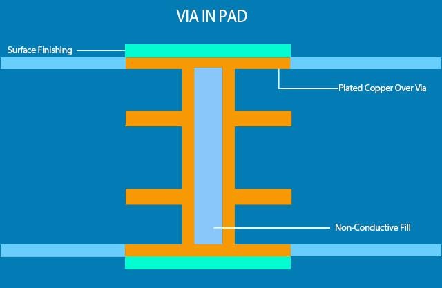
PCB via in pad can save space and shorten signal paths. It can also help with thermal transfer when used under thermal pads.
However, via-in-pad is not the same as placing a normal via under a pad. For reliable assembly, you usually need to fill and cap the via. If you do not do this correctly, solder may flow into the via during assembly.
PCB Via Tenting, Plugging, Filling, and Capping
Via treatment is also important. You can finish the same via in different ways based on soldering, assembly, and reliability needs.
Common treatments include:
- PCB via tenting
- Plugged via
- Filled via
- Capped via
These are not always “via types” in the layer connection sense. They are process choices that affect protection, soldering, and assembly quality.
PCB Via Tenting
PCB via tenting covers the via opening with solder mask. It helps protect the via from solder, dust, and other contaminants.
PCB via tenting can help:
- Reduce solder bridging
- Reduce dirt and debris
- Protect small vias
- Lower process cost
However, via tenting is not suitable for all via sizes. Large vias may remain partially uncovered. The solder mask may break or leave openings.
For critical products, ask the manufacturer if the via size is suitable for tenting.
Plugged Via
A plugged via is blocked with solder mask ink or resin. This helps stop solder, chemicals, or dirt from entering the via hole.
Plugging is more controlled than simple tenting. Designers use plugged vias to give the via stronger protection.
Plugged vias are useful when the board requires cleaner assembly or better process control.
Filled Via
A filled via is filled with resin or conductive material. Resin-filled vias are common in via-in-pad designs.
Filled vias can improve surface flatness. They can also help prevent solder from flowing into the hole.
For many PCB via in pad designs, filling is a key step before capping.
Capped Via
A capped via is usually a filled via that is plated over with copper. This creates a flat copper surface above the via.
Capped vias are useful for BGA pads and fine-pitch assembly. They help create a smooth pad surface for soldering.
This process costs more, but it improves assembly reliability in advanced PCB designs.
PCB Via Types Comparison Table
This table can help you compare options quickly. Still, the best choice depends on the PCB stackup, component layout, electrical needs, and production limits.
| PCB Via Type | Best For | Main Benefit | Main Limitation |
|---|---|---|---|
| Plated through-hole vias | Standard PCB designs | Low cost and reliable | Uses space on all layers |
| Blind vias | HDI PCB and BGA routing | Saves routing space | Higher cost |
| Buried vias | Dense multilayer PCB | Frees outer layers | Complex manufacturing |
| Microvias | Fine-pitch and compact PCB | High routing density | Needs advanced process |
| PCB via in pad | BGA and compact layout | Short signal path | Needs filling and capping |
| PCB via tenting | Small via protection | Low-cost protection | Not suitable for all via sizes |
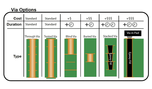
Different via types require different manufacturing processes. They also affect PCB cost and lead time. Simple vias are easier to produce and usually cost less. Advanced vias, such as blind vias, buried vias, microvias, and via-in-pad, need tighter process control and may require more production time.
PCB Via Design Rules to Check Before Manufacturing
Before sending files for PCB fabrication, check these via design rules:
- Minimum drill size
- Minimum annular ring
- Via aspect ratio
- Copper plating thickness
- Via-to-trace spacing
- Via-to-pad spacing
- Via current capacity
- Solder mask clearance
- Filled or capped via requirements
- Stackup and lamination limits
These rules can change based on PCB type, material, copper weight, thickness, and layer count.
Need Help with PCB Via Design?
Conclusion
The right PCB via type affects both layout design and manufacturing success.
HXD can review your Gerber files, stackup, drill table, material, copper thickness, and via structure before production. This helps reduce manufacturing risk and improve PCB reliability.
If your design includes HDI, BGA, high-speed signals, heavy copper, or compact routing, send your files for review before production.