2-Layer vs 4-Layer PCB: Which One Should You Choose?
Think Deeper with AI:
Introduction
Printed circuit boards(PCB) can have different layer counts depending on the circuit’s complexity and performance needs. 2-layer and 4-layer PCBs are the two most common types. Understanding their differences in structure, performance, and cost will help engineers choose the best solution for any electronics project.
What Is a 2-Layer PCB?
A 2-layer PCB, often called a double-sided PCB, has copper layers on both sides of an insulating substrate.
Its structure usually has three parts: a top copper layer, an insulating core (usually FR4), a bottom copper layer.
Because of limited routing space and weaker EMI shielding, 2-layer PCBs are not ideal for high-speed signals. Their primary applications include low-speed digital circuits, and budget-friendly consumer electronics.
What Is a 4-Layer PCB?
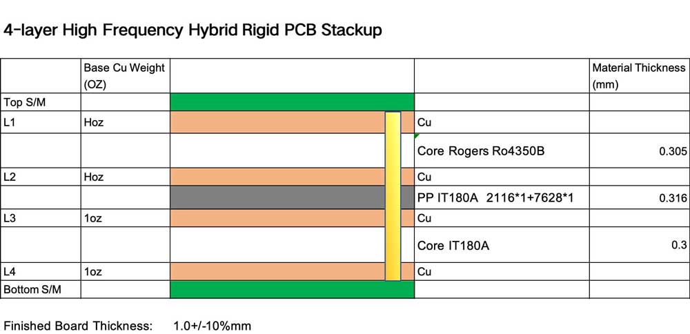
A 4-layer PCB is a multilayer printed circuit board that adds two internal layers for power and ground based on a double-layer PCB. It is commonly used in complex or high-speed electronic circuits. A typical structure is as follows:
- Top Layer: Signal layer for component placement and routing.
- Inner Layer 1: Ground plane. It provides a stable ground reference and return path.
- Inner Layer 2: Power plane. It distributes power and ensures stable voltage delivery.
- Bottom Layer: Signal layer for additional routing and component soldering.
A 4-layer PCB improves signal integrity, EMI shielding, and routing density, but costs more to manufacture.
You can use our Online PCB Stackup Design Tool to explore a range of preset 4-layer stackup templates.
Differences in Via Types
2-layer PCBs only support through-hole vias.
4-layer PCBs support blind and buried vias. These vias connect internal layers. They can also connect internal and outer layers. This flexibility makes it easy to handle complex routing for fine-pitch components like BGAs.
Differences in Impedance Control
Because of their thickness (typically 1.6mm), 2-layer PCBs make it difficult to achieve 50Ω or 100Ω impedance control.
In 4-layer PCBs, the insulation between the signal layer and the reference plane is much thinner. This makes it much easier to control both single-ended and differential pair impedance.
Signal Integrity and EMI Differences
On a 2 layer PCB, signals and return paths often share limited space. If a signal trace crosses a gap in the ground path, the return current must take a longer route. That larger loop can create more noise and more radiation.
On a 4 layer PCB, designers often use one inner layer as a solid ground plane. This gives signals a short and stable return path. It also reduces loop area.
Smaller loop area usually means lower EMI.
A 4 layer PCB also helps reduce crosstalk. Crosstalk happens when one signal couples into another signal. Dense 2 layer boards can make this worse because traces often run close together for long distances.
Impedance also matters. USB, Ethernet, RF, and other fast signals need more controlled routing. A 4 layer PCB gives engineers more predictable spacing between signal traces and the reference plane.
A well-designed 2 layer PCB can still pass EMI and work well. This is common for low-speed boards with short traces, clean grounding, and simple power needs. But once the layout becomes dense or noisy, 4 layers often reduce risk.
Is a 4-Layer PCB Better Than a 2-Layer PCB?
A 2 layer PCB can be the better choice for simple products. It costs less, has a simpler stackup, and allows easier visual inspection. Engineers can also debug many low-speed circuits faster on a 2 layer board.
Choose a 2 layer PCB when the board has:
| 2 Layer PCB Fit | Reason |
|---|---|
| Low-speed signals | Routing does not need strict impedance control. |
| Simple circuits | Fewer traces reduce layout pressure. |
| Large board space | Designers can route wider traces and better spacing. |
| Low component density | Parts do not force tight routing. |
| Basic power needs | Power and ground can route cleanly. |
| Cost-sensitive products | Lower fabrication cost matters. |
A 4 layer PCB becomes better when the design has clear limits. These limits may include dense routing, fast edges, EMI risk, ground return problems, or a small enclosure.
Choose a 4 layer PCB when the board has:
| 4 Layer PCB Fit | Reason |
|---|---|
| Dense components | Inner layers reduce routing pressure. |
| High-speed signals | Ground planes support cleaner return paths. |
| EMI concerns | Smaller loop areas reduce radiation. |
| Small board size | More layers allow tighter placement. |
| Mixed analog and digital circuits | Better grounding improves noise control. |
| Certification needs | Better structure can reduce EMC redesign risk. |
The practical rule is simple. Use 2 layers when the circuit is simple and quiet. Use 4 layers when the circuit needs stronger control.
2-Layer vs 4-Layer PCB Cost Comparison
The cost difference between 2-layer and 4-layer PCBs mainly comes from material usage, manufacturing processes, and production complexity. Since 4-layer PCBs require more copper layers and lamination, their overall cost is generally higher.
1. Material Cost
A 4-layer PCB requires additional inner copper layers, prepreg, and core materials. It uses more raw materials than a 2-layer PCB, so the material cost is higher.
2. Manufacturing Process
The production process of a 2-layer PCB is relatively simple. It mainly includes double-sided circuit fabrication, drilling, and plating.
A 4-layer PCB requires multilayer lamination and inner layer processing, which makes the process more complex. In most cases, the manufacturing cost of a 4-layer PCB is about 30%–50% higher than a 2-layer PCB.
3. Labor and Design Costs
Designing 4-layer boards requires expertise in signal integrity (SI), EMI, and impedance control, which can increase design costs by 2 to 3 times.
Quality inspection for 4-layer PCBs is also stricter. It may include inner-layer AOI inspection, layer alignment checks, and electrical testing. More inspection steps mean higher labor costs.
However, a 4-layer PCB includes dedicated power and ground planes, which can simplify routing. This may reduce layout design time by about 30%–50%. In many professional projects, the time saved by engineers can offset the extra manufacturing cost.
4. Long-Term Value and Hidden Costs
4-layer PCBs can reduce board size by at least 30% and support high-density components like BGAs. A smaller board saves money on the product enclosure and overall device size. In addition, 4-layer PCBs provide better heat distribution and stronger mechanical stability, which can significantly reduce maintenance and after-sales repair costs.
Need help choosing between a 2-layer and 4-layer PCB? Send us your Gerber files , our engineering team can help you review the stackup, and cost.
When Should You Choose a 4 Layer PCB?
In general, when design requirements increase, engineers often upgrade from a 2-layer PCB to a 4-layer PCB. The common reasons include the following:
1. Better return path and impedance control
A 4-layer board can provide a solid return plane that is separated from the signal layer by a thin dielectric layer. This structure makes it easier to control single-ended and differential impedance. It also provides a stable return path for high-speed signals and helps reduce EMI (electromagnetic interference).
2. Easier routing and component placement
When a circuit has many signal traces, adding more layers can greatly simplify PCB routing and component placement. If most components can be placed on the same side of the board, routing becomes much easier. In some cases, this design improvement can offset the extra cost of upgrading from a 2-layer board to a 4-layer board.
3. Reduced signal noise
A 4-layer PCB usually includes a solid ground plane. This helps reduce noise between different areas of the board and improves overall electrical performance.
4. Higher current carrying capability
Complex systems need steady power. Dedicated layers reduce power noise and ensure the system remains stable under load.
5. Better power distribution
Besides ground planes, split power planes can provide wider or thicker power paths for different voltage rails. This helps reduce IR drop (voltage drop) in power traces and improves power stability.
Conclusion
Choosing between a 2-layer and a 4-layer PCB is essentially about balancing project budget and circuit performance.
If your project is simple and cost is your top priority, a 2-layer PCB is the best choice.If you want better signal stability and a shorter development cycle, the long-term value and performance of a 4-layer PCB usually outweigh its higher initial cost.
If you are unsure which option fits your project, contact HXD Circuit. Our professional layer stack advice can help shorten development time and reduce mass production risks.
Send your Gerber files to us
We can help check your layer count, stackup, copper weight, and manufacturability before production.
Get StartedFAQ