sales@hxdcircuits.com
+86 180 1876 7219

Why Choose HXD 12-Layer PCB?

12Layer FR4 ISOLA 370HR Tg170

HXD has many years of mass production experience with 12-layer PCBs.We fully control the key manufacturing processes required for multilayer boards and consistently deliver high-reliability, complex PCB solutions.

Registration Accuracy

Accurate layer-to-layer alignment is critical in 12-layer PCB manufacturing.HXD uses laser registration systems to control layer misalignment within ±0.08 mm, effectively preventing pad and hole offset and ensuring reliable drilling and assembly.

High Aspect Ratio Plating

12-layer boards often require high aspect ratios of 12:1 or even 25:1. We optimize our plating formulas and parameters to ensure uniform copper thickness on hole walls without voids or cracks, meeting high-reliability requirements

Microvia & Laser Drilling

HXD supports blind vias, buried vias, and stacked vias for advanced interconnect designs.Laser drilling capability reaches a minimum via size of 3 mil (0.075 mm), supporting high-density and high-integration PCB designs.

Advanced Material Processing Capability

HXD processes a wide range of high-performance materials, including High-Tg (Tg170) FR-4, Rogers high-frequency materials, Polyimide, and hybrid laminate structures.These materials are suitable for high-speed, high-frequency, and harsh-environment applications.

PCB Certifications

HXD 12-Layer PCBs

12Layer FR4 ISOLA 370HR Tg170

12Layer FR4 ISOLA 370HR Tg170

Reliable Supply of ISOLA 370HR (Tg170),Industrial-Grade 12-Layer Stack-Up,High-Precision Conductive Performance

12Layer HDI with ISOLA 370HR Tg170

12Layer HDI with ISOLA 370HR Tg170

12-layer stackup with multiple HDI build-up (L1-2, L11-12) enables high-density routing, compact layouts, and advanced miniaturized designs.

Ready to start your 12-layer PCB project

Upload your Gerber files to get an instant quote.

Start Custom Quote

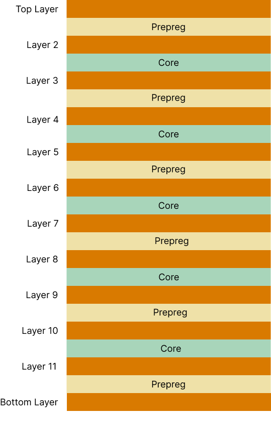
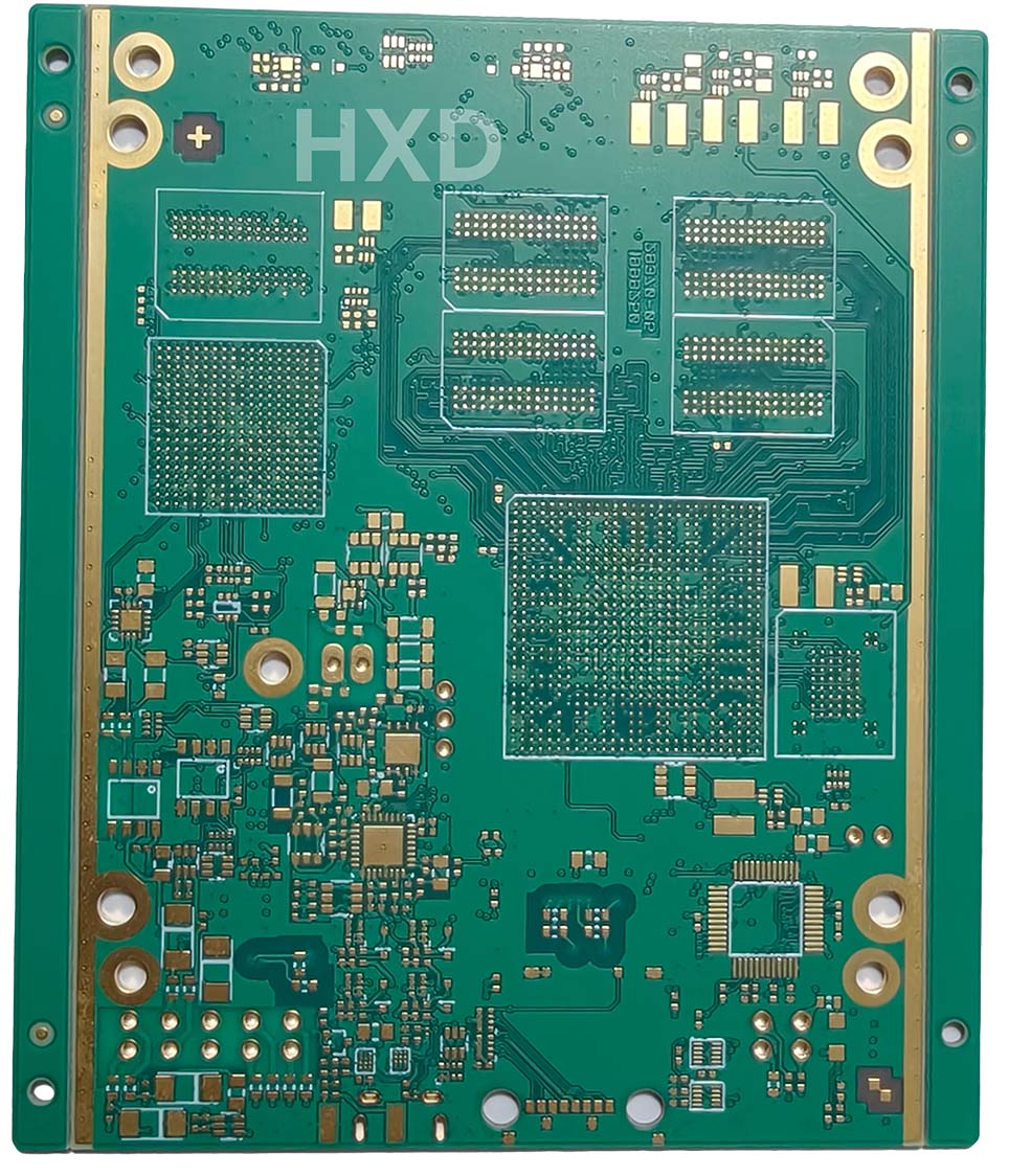
what is a 12-Layer PCB?

A 12-layer PCB is a multilayer printed circuit board made by stacking and laminating 12 layers of conductive copper foil. Each layer is separated by insulating dielectric materials.

Structure

The board typically consists of 2 outer layers (Top and Bottom) and 10 inner layers. These inner layers are strategically assigned as Signal, Ground, or Power planes to handle complex electrical connections and provide EMI shielding.

Materials

  • Copper: The conductive material used to transmit signals and power.
  • Prepreg: An insulating material that bonds the cores and copper foils together.
  • Core / Substrate: A rigid dielectric material with copper foil that provides structural support and insulation.

12-Layer PCB stackup

A 12-layer stack-up defines the vertical order of signal, power, and ground layers. A well-designed stack-up provides short return paths for signals, reducing Electromagnetic Interference (EMI) and crosstalk. By precisely controlling dielectric thickness, we manage controlled impedance to minimize signal reflection and distortion.

Core Principles of Stack-up Design:

  • Symmetry
    To control board warpage during reflow soldering, the stack-up must be physically symmetrical around the center line.

  • Adjacent Reference Planes
    Ideally, each signal layer should be placed next to a reference plane (ground or power) to shorten the current return path and lower impedance.
  • Material Selection
    For 12-layer and higher PCBs, high-Tg materials (such as Tg170) are recommended to prevent delamination or blistering during lead-free soldering and other thermal processes.

12-Layer Rigid PCB Stackup Case1

hxd-12-layer-pcb-stackup

Finished Board Thickness: 1.6+/-10%mm
Application: Industry Control
Layer: 12L
Material: ISOLA 370HR
Min.Line W/S: 0.067/0.175mm
Surface Finish: ENIG
Special Feature: Resin Plugging+Impedance Control
Impedance Tolerance Layer Reference Width/Spacing (mm)
Single ended impedance lines 50Ω ±10% L1 L2 0.1
Differential impedance pairs 100Ω ±10% L1 L2 0.1/0.175
Single ended impedance lines 50Ω ±10% L3 L2/L4 0.086
Differential impedance pairs 100Ω ±10% L3 L2/L4 0.08/0.195
Single ended impedance lines 50Ω ±10% L5 L4/L6 0.07
Differential impedance pairs 100Ω ±10% L5 L4/L6 0.067/0.2
Single ended impedance lines 50Ω ±10% L8 L9/L7 0.086
Differential impedance pairs 100Ω ±10% L8 L9/L7 0.067/0.2
Single ended impedance lines 50Ω ±10% L10 L9/L11 0.086
Differential impedance pairs 100Ω ±10% L10 L9/L11 0.08/0.195
Single ended impedance lines 50Ω ±10% L12 L11 0.1
Differential impedance pairs 100Ω ±10% L12 L11 0.1/0.175

When Do You Need a 12-Layer PCB?

Compared with a 10-layer PCB, a 12-layer PCB has higher cost and manufacturing complexity.Because of this, it is not a mainstream choice and is less common in real applications.

Engineers choose 12-layer structures only when project requirements for space utilization, signal integrity, and power stability are extremely high. Typical applications include:

1. Limited Board Space

A 12-layer board provides more routing surfaces without increasing the physical size of the PCB. This is common in compact devices like laptops and smartphones.

2. High Pin-Count Components (BGA)

When using components with high pin counts, such as a 324-pin BGA, routing can become congested. A 12-layer structure provides the extra layers needed for dense signal breakout and pad access.

3. High-Frequency & High-Speed Circuits

For systems running at high speeds (Ethernet, DDR, PCIe) or high frequencies (up to 100 GHz), a 12-layer stack-up offers dedicated reference planes. This significantly reduces impedance mismatch, timing jitter, and crosstalk.

4. Signal Isolation

A 12-layer design allows for the physical separation of analog signals, digital logic, and Radio Frequency (RF) on different layers. This ensures multiple signal types can coexist without interference.

REQUEST A QUOTE

Supported file formats: PDF, DOC, DOCX, TXT, JPG, PNG (Max 2MB)