sales@hxdcircuits.com
+86 180 1876 7219

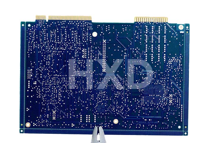
When to Use an 8-Layer PCB?

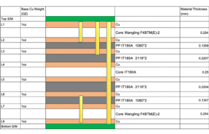
An 8-layer PCB comprises 8 layers of copper, each separated by a layer of insulating material (Prepreg and Core). It is a high-end PCB. Typically, 8-layer PCBs are used for projects with extremely high requirements for signal speed, power handling, and electromagnetic shielding. Specifically, 8-layer PCBs are suitable for the following scenarios:

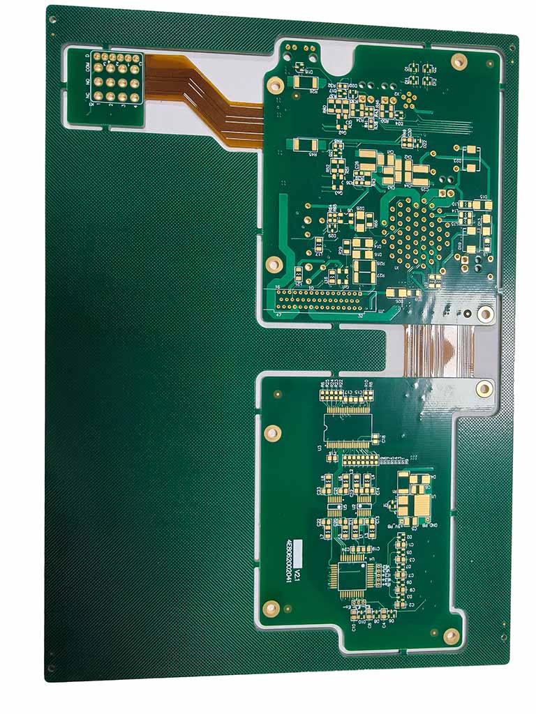
  • High-Density Design:When your product needs to integrate many components and complex routing in a limited area, an 8-layer structure provides enough routing layers to carry these circuits. It is especially suitable for micro-electronics and wearable devices. If your design involves multiple different Power Islands, an 8-layer PCB  provides sufficient space for routing and ensures isolation between different  subsystems.
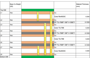
  • Strict Requirements for Signal Integrity (SI):The stackup of an 8-layer board is symmetrical. This structure effectively controls impedance accuracy and supports the stable transmission of high-speed signals above 28Gbps. In addition, the design usually places signal layers next to ground or power planes. This can reduce crosstalk between signals by over 30% and provide a clear return path.
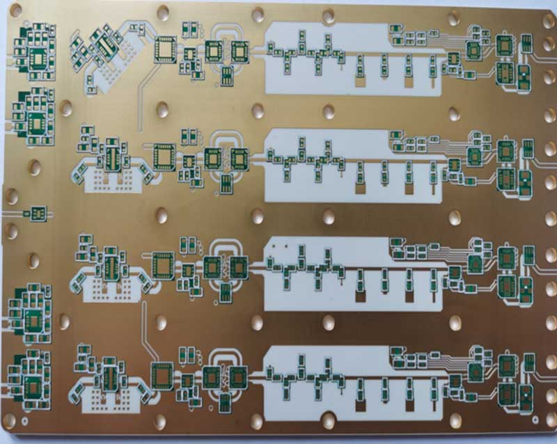
  • High Requirements for EMC/EMI:By adding multiple ground and power planes, an 8-layer PCB acts as a shield for internal signal layers. This structure can significantly reduces Electromagnetic Interference (EMI). If your device needs to operate in environments with strong radiation or complex electromagnetic noise, the 8-layer structure provides powerful anti-interference capability.
  • Thermal Management:The dedicated power planes of an 8-layer PCB can handle high current above 10A. When working with high voltage above 500V, the multilayer structure provides better interlayer insulation and creepage distance, reducing the risk of electrical arcing.When your product includes high-power components, such as MOSFETs with power dissipation above 5W and strict thermal requirements, an 8-layer PCB uses large internal copper areas and thermal vias to dissipate heat more effectively.

PCB Certifications

HXD 8-Layer PCBs

HXD has extensive experience in 8-layer PCB manufacturing. We have successfully delivered many complex 8-layer PCB products. Below are some typical 8-layer PCB cases for your reference.

8Layer FR4 Tg170

8Layer FR4 Tg170

Our hard gold fingers are plated with a thick 40μ” of gold, specifically designed to withstand thousands of mating cycles without wear, ensuring long-term reliability.

8Layer Rigid-flex PCB with Dupont AP8535R and Arlon 49N

8Layer Rigid-flex PCB with Dupont AP8535R and Arlon 49N

Advanced 8-Layer Rigid-Flex Stackup,hybrid Laminating Expertise

Ready to start your 8-layer PCB project

Upload your Gerber files to get an instant quote.

Start Custom Quote

8 Layer PCB Stackup Overview

8-LAYER PCB STACKUP

There are several stackup options for 8-layer PCBs. Different stackups are designed for different applications.

  • Signal Layers:The internal signal layers provide extra routing space for complex circuits and support high-density component placement. To reduce crosstalk, the routing direction of two adjacent internal signal layers should be perpendicular to each other.
  • Ground Planes:Ground planes provide a clear and low-impedance return path for signals. Without a well-defined return path, signals will create serious EMI. As a reference plane, the ground plane allows for precise impedance control (up to ±5%) by matching the spacing and material properties.
  • Power Planes:Power Planes provide a stable power supply for all components on the PCB. They also act as a shield for signal layers, helping to reduce crosstalk between layers.


The following are HXD’s commonly used 8-layer PCB stackups,You can also explore our Flex PCB Stackup  and   rigid-flex PCB stackup options.

HXD High Frequency Hybrid Rigid PCB+HDI

High-Frequency-Hybrid-Rigid-PCB+HDI

Finished Board Thickness: 1.65+/-10%mm
Application: 5G Massive MIMO
Layer: 8L
Material: Ro4003+Tu-768
Surface Finish ENIG

High Frequency Hybrid Rigid PCB+HDI Product Img

HXD PTFE Hybrid Rigid PCB+HDI

PTFE Hybrid Rigid PCB+HDI

Finished Board Thickness: 1.8+/-10%mm
Application: Advanced Radar Systems
Layer: 8L
Material: F4BTM(E)+IT 180A
Surface Finish: ENIG
Comment: The material lead time for Alon/Teflon is long and the price is very expensive.
Wangling is Chinese brand and can use to replace some of the P/N

FAQ

What factors affect the cost of an 8-layer PCB?

  • Materials: Rogers or ceramic substrates are much more expensive than standard FR-4.
  • Hole Size and Quantity: Extremely small holes or Blind/Buried Vias require special processes and more drilling time.
  • Surface Finish: HASL is the most affordable option, while ENIG or ENEPIG costs more.
  • Board Size and Copper Thickness: Large dimensions or Heavy Copper (thick copper) will significantly increase material costs.

What impedance tolerance can an 8-layer PCB achieve?

The impedance tolerance of an 8-layer PCB can usually reach ±5%.This is critical for supporting 28Gbps+ high-speed signals and for interfaces such as DDR4 and DDR5.

What materials are commonly used for 8-layer PCBs?

FR-4 Tg170,Rogers 4350B, Megtron 6, Polyimide

What is the standard thickness of an 8-layer PCB?

The total thickness of an 8-layer PCB is usually between 1.57mm and 2.36mm. However, in actual applications, the thickness can be customized from 1.0mm to 5.0mm. The final thickness depends on your choice of materials, copper thickness (usually 1oz or 2oz), and lamination parameters.

REQUEST A QUOTE

Supported file formats: PDF, DOC, DOCX, TXT, JPG, PNG (Max 2MB)