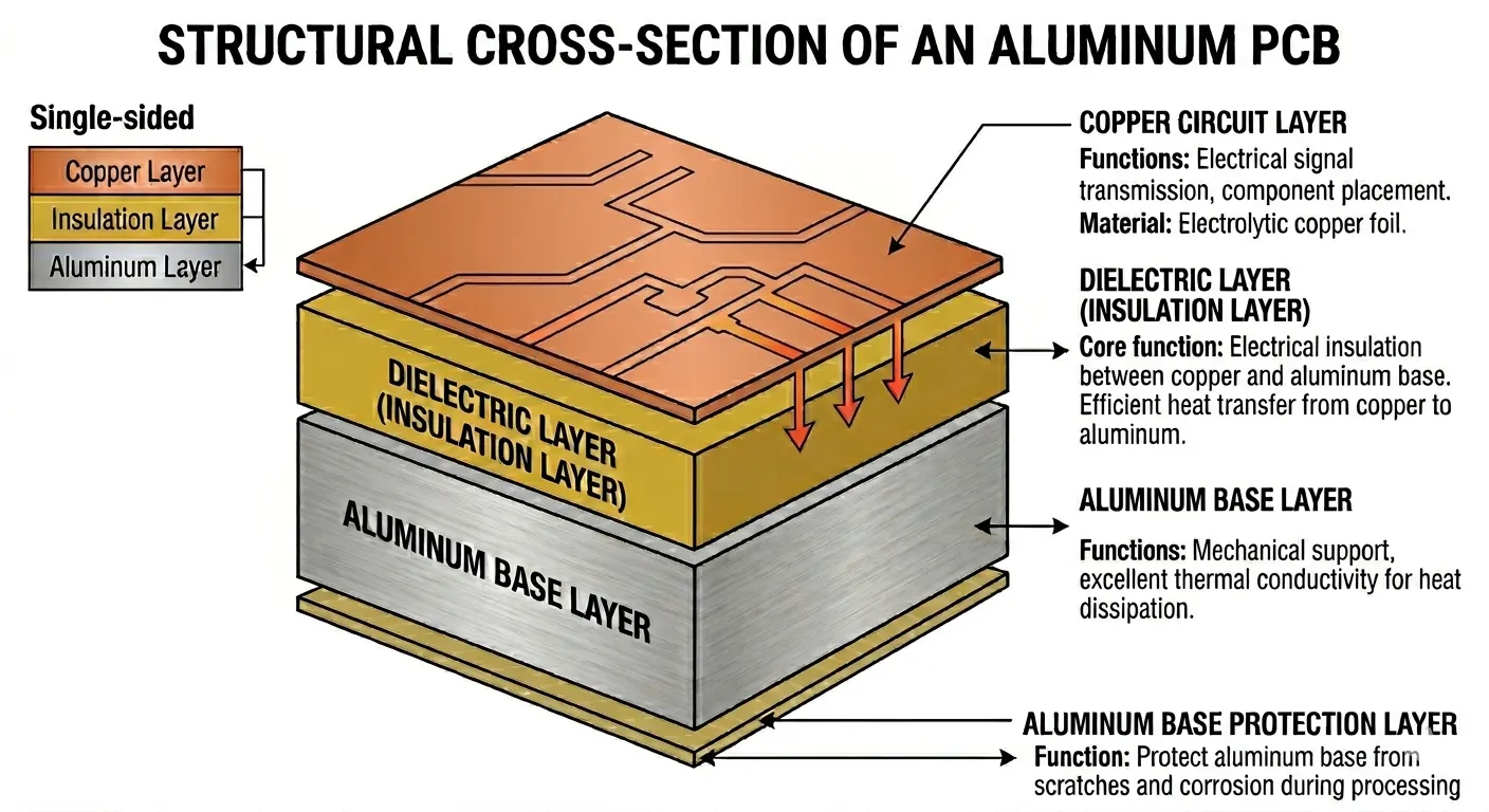
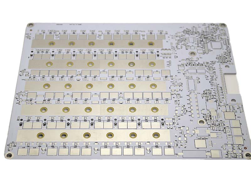
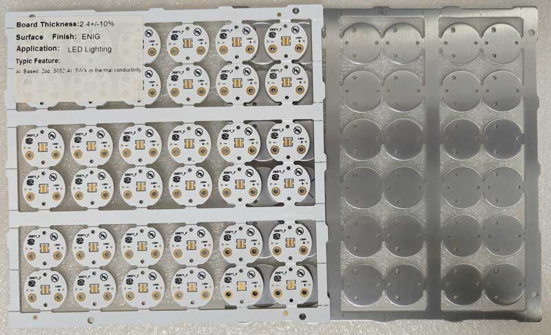
HXD's Manufacturing Capabilities
Compared to traditional PCBs, aluminum substrates are much more difficult to process. It must rely on more sophisticated production equipment for core processes such as drilling, etching and solder mask printing. In the core processes, it is necessary to rely on more sophisticated production equipment. HXD has many years of experience in aluminum substrate production, with the ability to control the whole process from material selection, production, to finished product testing:
- Layer support: 1-6 layers of aluminum substrate.
- Maximum size: up to 1500 × 540 mm.
- Surface treatment: HASL (leaded/lead-free), ENIG (immersion gold), OSP.
- Precision machining: Supports blind via,buried via, insulated slotted, Countersink Hole, Z-axis milling, and Pedestal structures.
- Quality inspection: including appearance inspection, thermal shock test, board flatness test, high voltage test.
We can design different structures based on your requirements.
- Double-sided Aluminum PCB: Wired on both sides, with the space between the holes filled with resin to achieve insulation, suitable for electronic products with certain requirements for thermal management and more complex circuit logic.
- Single/double-layer Aluminum PCB: the most common, simplest to manufacture, and suitable for basic thermal management needs.
- Multi-layer Aluminum PCB: more difficult to manufacture, in very high density design, the overall thermal conductivity compared to single/double layer has decreased.