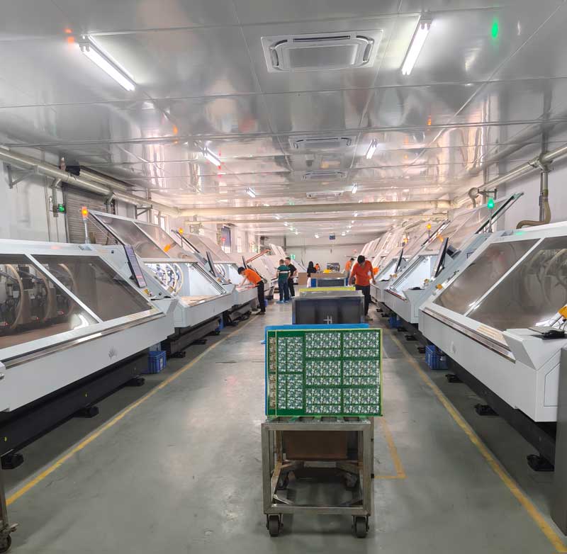
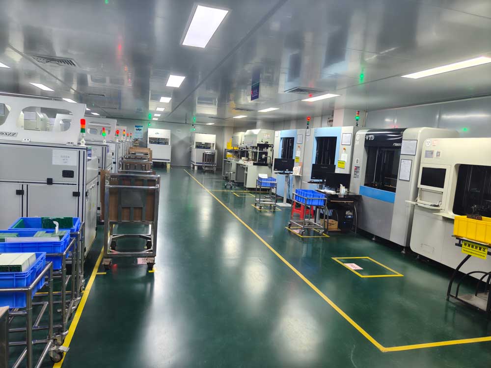
PCBs Manufacturing Process at HXD:Step-by-Step Guide
A standard PCB manufacturing process can let everyone understand simple PCB layer and multilayer PCB easily. Let’s give you a Step-by-Step Manufacturing Overview in HXD production line.
Step1 – PCB Design & Engineering Review
The process starts with your PCB design files (Gerber, drill files, stack-up). Our engineers review the design to ensure it is manufacturable within HXD production capability and meets electrical, mechanical, and reliability requirements.
If an engineering issue happens, the whole batch will have quality issues. A professional engineering review in HXD helps avoid costly issues later, such as impedance mismatch, layer misalignment, or manufacturing risks.
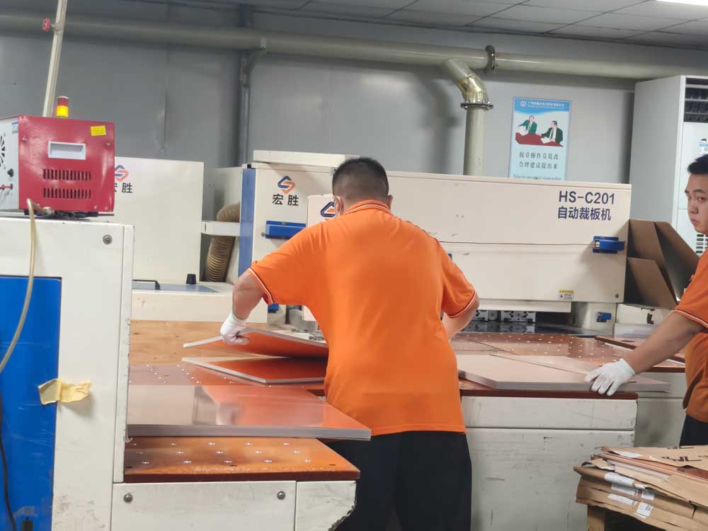
Step2 – Material Cutting
Large copper-clad laminate panels are cut into production-sized sheets according to the Manufacturing Instruction.
Accurate cutting ensures consistent panel size, improves process stability, and improves material utilization. It’s an important process to control the PCB cost.
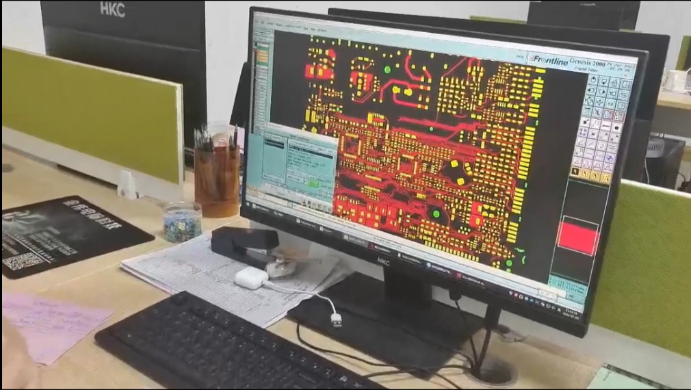
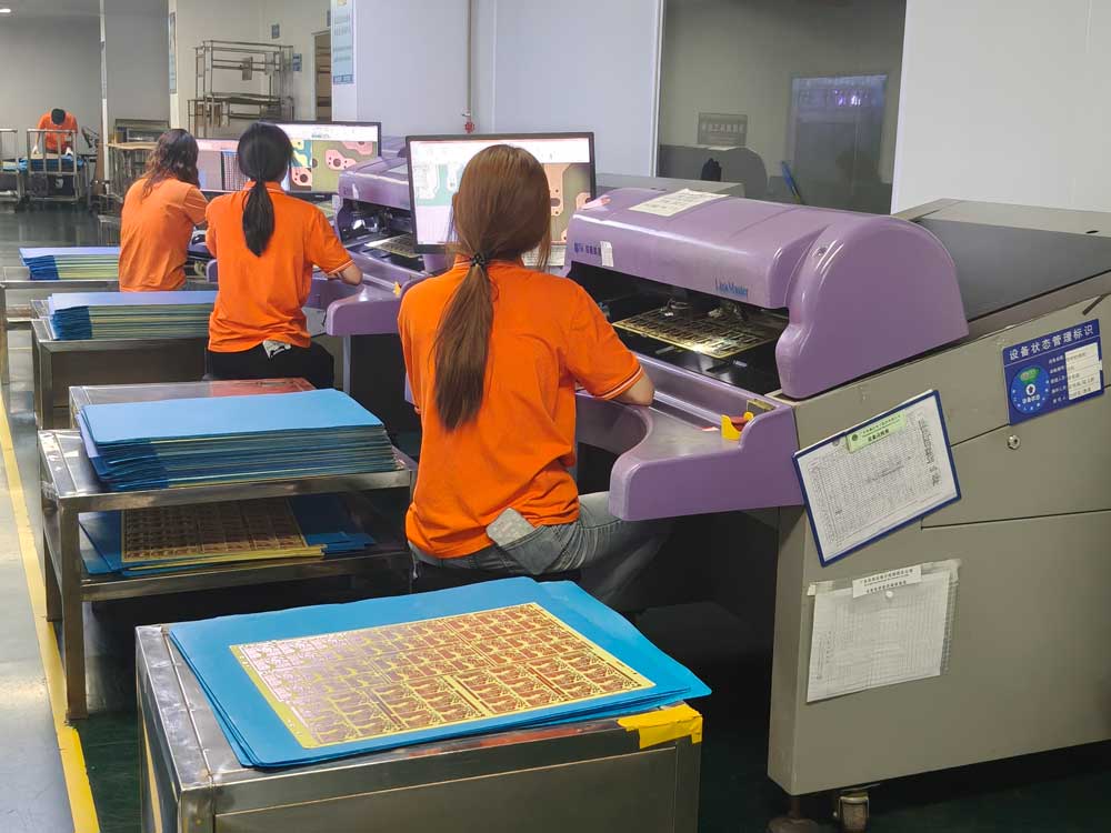
Step3 – Inner Layer Imaging
The copper layers that form the inner circuits (Layer 2 & Layer 3) are laminated with photoresist, exposed with the circuit pattern, and developed to reveal the copper traces.
Inner layers define the signal integrity and power distribution of a 4-layer PCB. Accuracy here is critical.

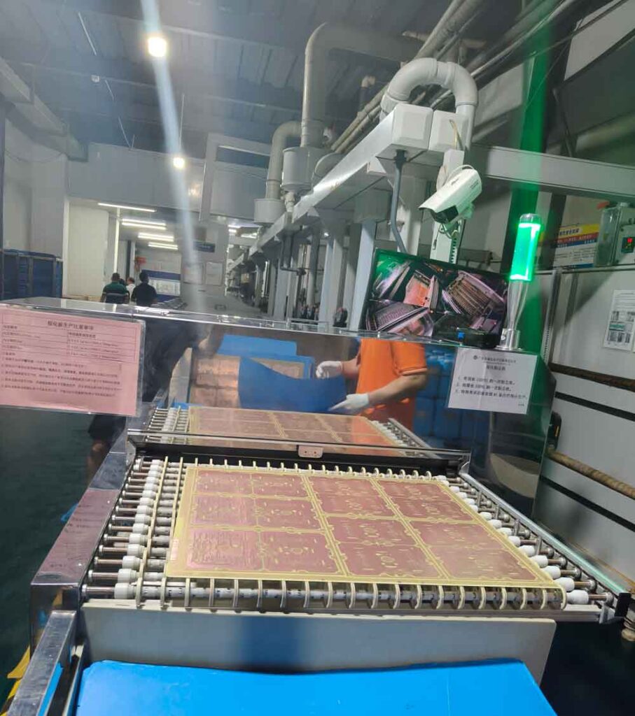
Step4 – Inner Layer Etching
Unwanted copper is chemically etched away, leaving only the required circuit patterns on the inner layers. To increase the board adhesive, the layers have brown oxidation before laminating process.
Clean and precise etching ensures correct line width, spacing, and electrical performance.
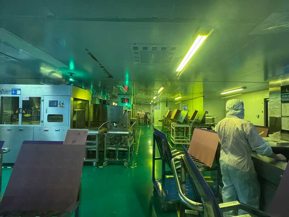
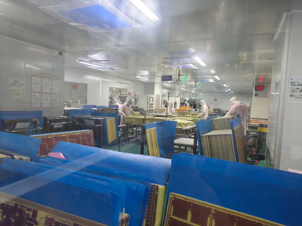
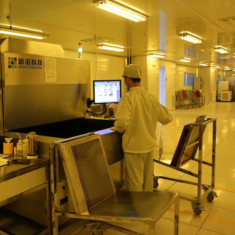
Step5 – Inner Layer Inspection
Each inner layer is inspected using Automated Optical Inspection (AOI) to detect shorts, opens, or missing copper.
Once layers are laminated together, defects cannot be repaired. This step ensures inner layer quality before proceeding.
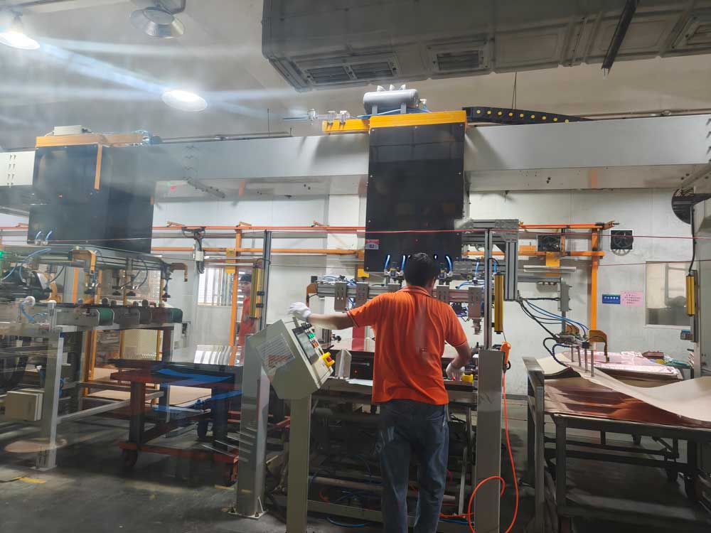
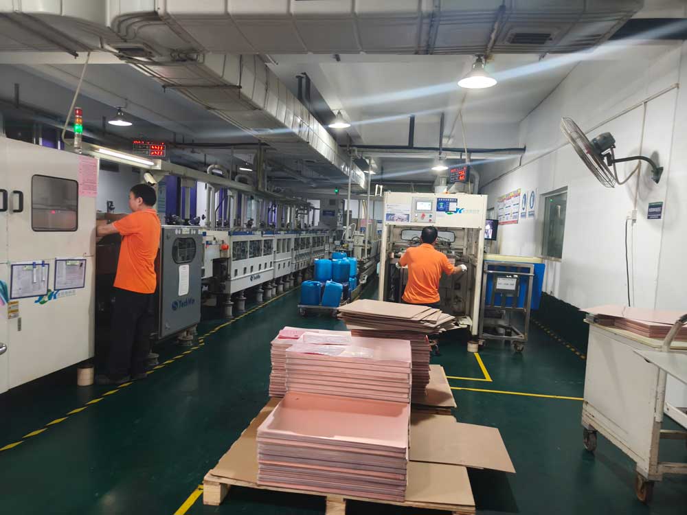
Step6 – Layer Stack-up & Lamination
The inspected inner layers are stacked with prepreg and copper foil, then pressed under high temperature and pressure to form a solid multilayer board.
Proper lamination ensures strong bonding, correct thickness, and long-term reliability.
Step7 – Drilling
Precision drilling creates holes for vias and component leads according to the design.Accurate drilling is essential for reliable electrical connections between layers.
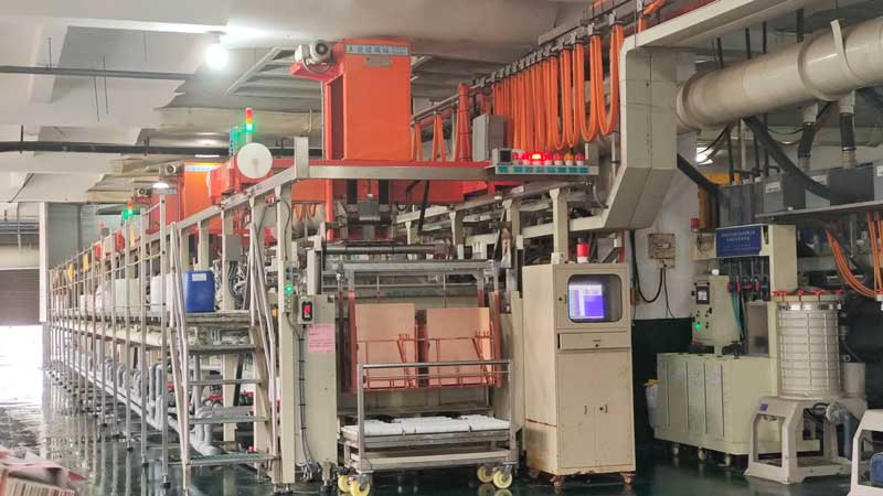
Step8 – Plated Through Hole
The drilled holes are chemically cleaned and plated with copper to create conductive connections between layers. PTH forms the electrical backbone of a multilayer PCB.
Step9 – Outer Layer Imaging
The outer layers (Top & Bottom) are imaged using LDI Exposure machine to transfer the circuit pattern.The signal integrity of the external layer of a 4-layer PCB is formed. Accuracy here is critical.
Step10 – Outer Layer Etching
Excess copper is removed, leaving the final circuit pattern on the outer layers.Precise etching ensures stable soldering and reliable signal transmission.
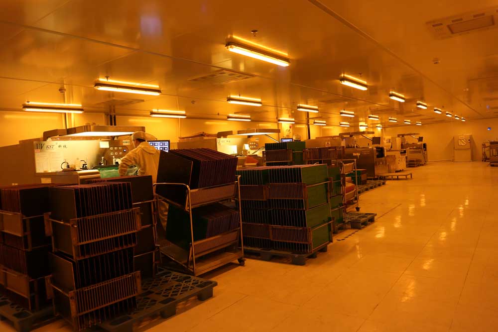
Step11 – Solder Mask Application
A solder mask layer is applied to protect copper traces and prevent solder bridging during assembly. It primarily serves as an insulating layer and protect the PCB’s electrical performance. Normally the colour will be green, white or black. Some other kinds of colours are also available, such as blue, red, purple, orange etc.
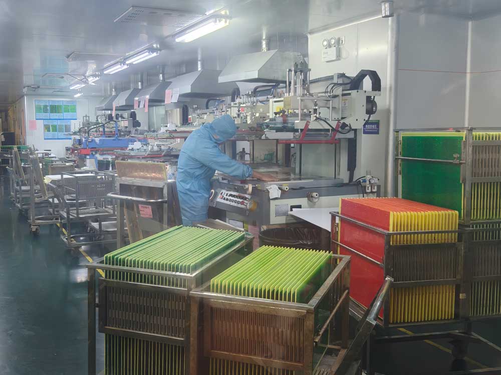
Step12 – Silkscreen Printing
Component markings, reference designators, and logos are printed onto the PCB surface. Clear silkscreen helps during assembly, inspection, and future maintenance.
Step13 – Surface Finish
A surface finish (such as ENIG, HASL, or OSP) is applied to exposed copper pads. Surface finish protects copper from oxidation and ensures good solderability.
Step14 – PCB Profiling (V-Cut & Routing)
The PCB is separated from the production panel using V-cut and/or CNC routing according to the required board outline.:
Accurate profiling ensures correct board dimensions, smooth edges, and compatibility with automated assembly processes.
Step15 – PCB Cleaning (After Routing)
After routing, the boards are cleaned to remove dust, resin residue, and contaminants generated during the profiling process.
Proper cleaning prevents contamination, improves surface cleanliness, and ensures stable electrical performance and long-term reliability.
Step16 – Electrical Testing (E-Test)
Each PCB is electrically tested to ensure there are no shorts or open circuits. This guarantees that every delivered board functions as designed.
Step17 – Final Inspection & Packaging
Boards will undergo final visual inspection per customer’s SPEC and IPC standard, dimensional checks, and are carefully packaged for shipment.
Proper inspection and packaging protect quality until the PCB reaches your hands.
written by
steve ran
Senior Layout Manager