The Difference Between HDI (High Density Interconnect) Boards and Traditional PCBs (Printed Circuit Boards)
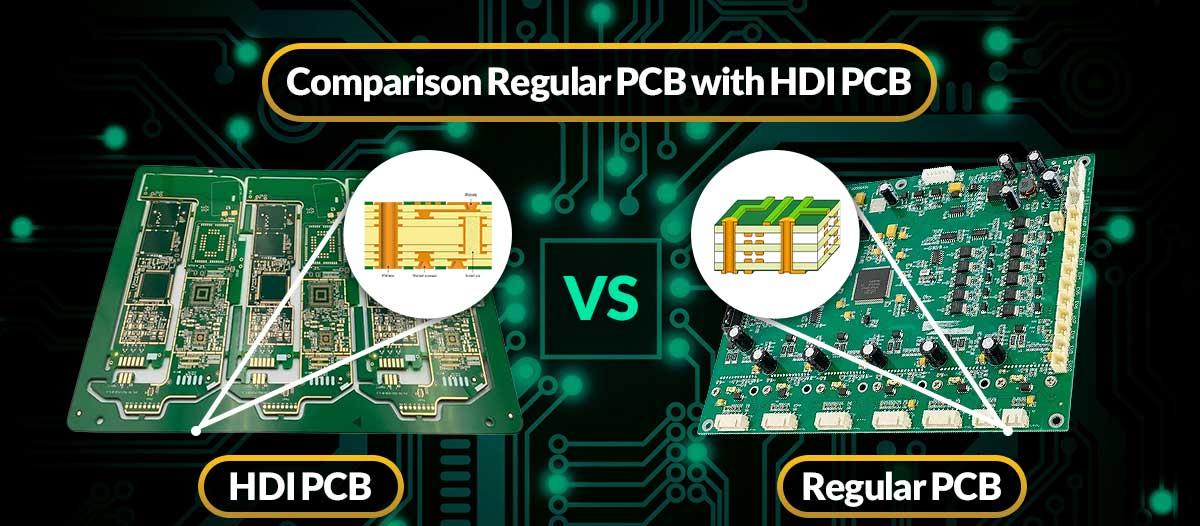
The primary difference between HDI (High Density Interconnect) boards and traditional PCBs (Printed Circuit Boards) lies in several key aspects, which contribute to the advanced performance and functionality of HDI boards. These differences are outlined below:
Density
HDI boards offer significantly higher line density compared to traditional PCBs, achieved through advanced design techniques. These techniques include:
- Fine line creation
- Blind and buried hole applications
- Efficient inter-layer connection technologies
These innovations enable HDI boards to fit complex circuits and components into a very small area, greatly enhancing the integration and functionality of electronic devices. This high density makes HDI boards ideal for applications requiring compactness and high performance.
Trace Width and Spacing
One of the standout features of HDI boards is the precision with which trace width and spacing are designed. The traces on HDI boards can be as fine as 4-6 mils (thousandths of an inch), which significantly reduces signal interference and improves signal transmission quality.
In contrast, traditional PCBs, often limited by technology and material constraints, require wider trace widths and spacings, which restrict their use in high-density, high-performance electronic devices. The precision offered by HDI boards ensures better performance in compact, high-frequency circuits.
Layer Count
HDI boards make use of multi-layer designs to enhance both wiring density and space utilization. By increasing the number of layers and optimizing the connections between layers, HDI boards can support complex circuit layouts while improving the board’s stability and reliability. This makes HDI boards particularly competitive in devices that require miniaturization and high integration.
Blind and Buried Hole Technology
HDI boards extensively use blind and buried hole technologies, which allow for direct connections between internal layers of the circuit board without passing through the entire board. This technology has several key benefits:
- Space savings: Reduces the need for through-holes, freeing up space for additional circuits.
- Increased circuit density: Facilitates a more compact layout with efficient connections.
- Simplified assembly: Streamlines the manufacturing process and reduces complexity.
These features make HDI boards particularly important for electronic devices that demand extreme compactness and efficient connections.
Technical Requirements
Given the high density and complexity of HDI boards, their manufacturing and assembly processes require advanced technical standards. These include:
- High-precision laser drilling
- Advanced electroplating processes
- Precise assembly and testing techniques
To ensure high product quality and reliability, HDI boards also require more advanced production equipment and strict quality control procedures throughout the manufacturing process.
Conclusion
HDI high-precision boards, with their high density, miniaturization, multi-layer design, and complex manufacturing requirements, have become the preferred choice for creating high-quality, advanced electronic devices. As technology continues to push the boundaries of miniaturization and performance, HDI boards will remain at the forefront of the electronics industry.
written by
steve ran
Senior Layout Manager