Ultimate Guide to Copper Thickness
Copper is the most critical material in a printed circuit board (PCB). Its heat dissipation capability is more than 1,000 times higher than that of FR-4. It also carries electrical signals efficiently with very low resistance. Copper thickness directly affects current capacity, thermal performance, and manufacturing processes. This article explains how to choose appropriate copper thickness in PCB design, helping engineers make proper decisions for different applications.
What Is 1oz Copper Thickness and How to Convert oz to μm?
In the PCB industry, the thickness of copper is usually expressed in “oz”,which stands for ounces. Why Use Weight to Measure Copper Thickness?This comes from a long-standing convention in PCB manufacturing. In early PCB production, it was difficult to directly measure copper foil thickness in millimeters or microns.
Measuring the weight of copper over a known area was much easier and more accurate.
By definition, if 1 ounce (28.35 grams) of copper is evenly spread over an area of 1 square foot (ft²), the resulting copper thickness is about 1.37 mil (approximately 34.8 µm).
Based on this relationship, common PCB copper thickness options such as 0.5 oz, 1 oz, 2 oz, and 3 oz were established.The table below shows common copper thickness conversions used in PCB design, allowing engineers to quickly select the appropriate copper weight.
| Copper weight(oz) | Copper thickness |
| 1 | 34.8µm/1.37mils |
| 1.5 | 52.20µm/2.06mils |
| 2 | 69.6µm/2.74mils |
| 3 | 104.39µm/4.11mils |
| 4 | 139.19µm/5.48mils |
| 5 | 173.99µm/6.85mils |
| 6 | 208.79µm/8.22mils |
| 7 | 243.59µm/9.59mils |
| 8 | 278.38µm/10.96mils |
| 9 | 313.18µm/12.33mils |
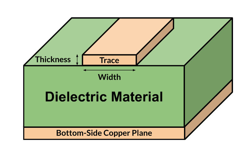
The relationship between copper thickness and trace width
Trace width and copper thickness are never independent parameters, they jointly determine the conductor’s cross-sectional area, which directly affects the trace resistance, temperature rise, and current carrying capacity.
The conductor cross-sectional area can be expressed as:
A = Trace Width x Thickness
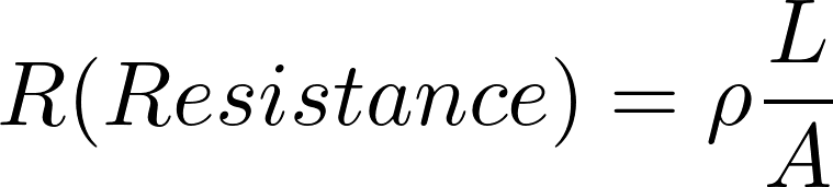
When the copper thickness or trace width increases, the cross-sectional area increases, and the resistance decreases. With the same current , less heat is generated. In short, wider trace and thicker copper usually provide higher current capacity and lower temperature rise.
is thicker copper always better? Not necessarily. According to extensive IPC-2152 test data, if you increase the cross-section mainly by adding copper thickness, you must actually reduce (derate) the current to maintain the same temperature rise. This effect is especially significant at higher temperature rises, such as 45°C.
Why is this? Because heat dissipation is not just about cross-sectional area; it depends more on the surface area.Even with the same cross-sectional area, different copper weights perform differently:
1oz Trace: It is wide and thin, providing a very large surface area to touch the air and the PCB substrate. This allows it to cool down very fast.
3oz Trace: It is like a “tall wall.” Although it has the same cross-sectional area, its top surface is much narrower. This smaller total surface area causes heat to build up more quickly.
The Bottom Line: If space allows, a “Wide Trace + Moderate Copper” design usually cools better than a “Narrow Trace + Ultra-Thick Copper” design.
When designing for current capacity, you should not only focus on increasing copper thickness. A more reasonable and reliable approach is:
- Prioritize Trace Width: Always increase the trace width first to improve current carrying capacity whenever possible.
- Use Heavy Copper Strategically: Only introduce heavy copper in space-constrained or high-current areas. Keep standard copper thickness for signal and low-power regions.
- Balanced Design: Treat trace width, copper thickness, temperature rise, and manufacturing feasibility as a single, integrated system.
This design philosophy—centered on thermal management and manufacturability (DFM)—helps you find the perfect balance between performance, cost, and lead time.
Why should the outer layers have the same copper thickness?
In the PCB manufacturing process, both outer layers (Top and Bottom) enter the etching machine at the same time. If the two sides use different copper weights—for example, 2 oz on the top and 1 oz on the bottom—the 2 oz side will require a much longer time to etch.
If the same process conditions are used for both sides, it will result in over-etching on the thinner 1 oz side.This asymmetrical design not only causes the PCB to warp or twist like a “potato chip,” but also significantly increases manufacturing costs. To protect the precision of fine traces, the starting copper thickness on both sides must be consistent.
How to Choose PCB Copper Thickness?
Based on our engineering and manufacturing experience, we recommend the following copper weights for different applications:
- Standard Designs: 1 oz is the most common standard copper thickness used by PCB manufacturers. It has a mature process and lower cost. Most consumer electronics products use 1 oz copper.
- High Current Requirements: Power modules and driver circuits should use 2 oz to 4 oz (or more). This is known as “Heavy Copper,” which helps reduce resistance and heat buildup.
- High-Frequency Signals: For GHz-level signals, “Skin Effect” causes current to flow primarily along the surface of the conductor. In these cases, copper surface roughness is often more critical than thickness. Generally, 0.5 oz to 1 oz is better for signal integrity control.
- Flexible Circuits (FPC): For circuits that require repeated or dynamic bending, thinner copper foils like 1/3 oz or 0.5 oz are preferred to achieve better flexibility.
Copper Thickness in Multilayer PCBs
In multilayer PCBs, different layers can have different copper thicknesses. For example, the outer layers may use 2 oz copper, while inner layers use 1 oz copper. However, mirrored layers should use the same copper thickness. In a 4-layer PCB, the top layer (L1) and bottom layer (L4) should have the same copper thickness. The inner power and ground layers (L2 and L3) should also be balanced.This symmetry ensures even heating during etching, lamination, and other high-temperature processes. It helps prevent board warpage and twisting caused by uneven copper distribution.
Conclusion
Copper thickness is never a simple “the thicker, the better” choice. You must find the right balance between electrical performance, thermal management, and manufacturing cost.
In real-world projects, copper requirements vary significantly depending on the application. Before finalizing your design, we strongly recommend evaluating your layout with a PCB manufacturer to ensure it meets their DFM (Design for Manufacturing) capabilities.
Why Does a Heavy Copper PCB Require Larger Line Spacing?
The thicker the copper layer, the more difficult the etching process becomes.
If the line spacing is too small, the etching solution may not fully remove the copper between traces.This can leave copper residue and cause short circuits. As a general rule, the line spacing should be at least three times the trace width.
Why Is Copper Better Than Aluminum in High-Current PCB Applications?
Although aluminum is conductive, copper is the preferred material in PCB manufacturing for several reasons.
-
- Thermal performance:
Copper has lower electrical resistance and higher thermal conductivity.
Its coefficient of thermal expansion (CTE) also matches PCB base materials more closely. - Solderability:
Copper is easy to solder.
Aluminum is difficult to use for standard SMT processes in PCB manufacturing. - Corrosion resistance:
In humid environments, copper is less chemically reactive.
It is more resistant to corrosion than aluminum.
- Thermal performance:
Does Increasing Copper Thickness Improve Signal Quality in High-Frequency Circuits?
Not necessarily. In high-frequency (GHz-level) applications, current flows mainly on the surface of the conductor due to the skin effect.
At 10 GHz, the skin depth of copper is only about 0.66 µm.This means increasing copper thickness provides little benefit in reducing high-frequency loss.
In contrast, copper surface roughness has a much greater impact on signal integrity.For this reason, high-frequency designs usually use 0.5 oz or 1 oz low-roughness copper foil, such as RTF or VLP copper.
Does Heavy Copper Significantly Affect the Final PCB Thickness?
Yes. Each heavy copper layer adds to the total board thickness.
In addition, more solder mask or prepreg is often required to cover thick copper traces. If the impact of copper thickness is not considered early in the design, the final board thickness may exceed tolerance.This can cause problems during enclosure or mechanical assembly.
written by
steve ran
Senior Layout Manager