sales@hxdcircuits.com
+86 180 1876 7219

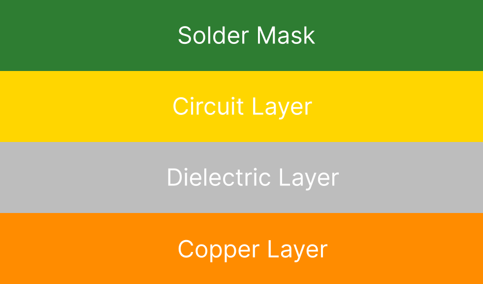
Why Choose HXD as Your Copper Core PCB Manufacturer?

Thermoelectric Separation  Technology: HXD utilizes an advanced process  to allow the thermal pads to have a “zero distance” connection to the copper substrate. This structure provides thermal performance near the physical limit for high power products.

 Pedestal Technology: We have high-precision copper etching technology to produce raised copper structures. Components can be mounted directly on the copper core. This greatly improves heat transfer and provides excellent grounding and signal stability.

All surface finishes are available: ENIG, silver, HASL and OSP.

PCB Certifications

HXD‘s Copper Core PCBS

10Layer coil PCB with thick copper weight

10Layer coil PCB with thick copper weight

Designed specifically for high-power industrial applications, ensuring reliable performance under demanding conditions.

1Layer Copper based PCB with Pillar Technology

1Layer Copper based PCB with Pillar Technology

Copper Core for Extreme Heat Dissipation Designed for high-power lighting applications, offering exceptional thermal conductivity up to 400 W/m·K, far beyond standard aluminum MCPCBs.

4Layer with Rogers+FR4 Hybrid Board+Copper Coin Buried

4Layer with Rogers+FR4 Hybrid Board+Copper Coin Buried

Hybrid Material: FR4 Tg170 + Rogers 4350,4-Layer Rigid Structure for Broadcasting Applications,High-Precision PCB Capability

led-pcb-copper

What is Copper Core PCB?

Copper Core PCB belongs to a kind of Metal Core PCB. Its substrate is made of pure copper material instead of common glass fiber (such as FR-4). Copper has very high thermal and electrical conductivity, superb thermal conductivity and excellent heat resistance in high power and high temperature environments.

copper core pcb stackup

Copper Core PCB Stackup Structure

Copper Core PCBs are typically composed of the following layers:

  • Solder Layer: Used for component soldering;
  • Circuit Layer: composed of copper foil, used to carry the circuit, copper weight is usually in the range of 1-10 oz;
  • Dielectric Layer: responsible for absorbing heat generated by the circuit layer and transferring it efficiently to the substrate while providing electrical isolation;
  • Copper Layer: absorbs and transfers heat from the circuit layer to the copper substrate for rapid diffusion.

This structure gives PCBs a significant advantage in thermal management.

Key Advantages of Copper Core PCBs

Superior Thermal Management

Copper has significantly better thermal conductivity than aluminum and iron, quickly transferring heat away from critical components and reducing reliance on external heat sinks.

Higher Durability and Reliability

Copper substrates are mechanically strong, less susceptible to deformation or corrosion due to thermal expansion and contraction, and significantly more resistant to thermal aging than ceramic or fiberglass PCBs.

Suitable for Direct Soldering of Components

Copper substrates support PTH and can be machined into raised structures for direct component placement.

Green and Recyclable

Copper is a natural material that is 100% recyclable, contributing to the environmental attributes of the project.

Get started with your next project

We can turn your standard technology PCBs in as fast as in 48 hours.
Start Custom Quote

Copper Core pcb VS Aluminum PCB

The table below allows you to visualize the core differences in physical properties and application costs between Aluminum PCBs and Copper Core PCBs. If you have questions about specific processing parameters, please feel free to contact Our engineers.

Properties Aluminum Copper Comments
Thermal Conductivity 1W – 3W/m·K 380- 400W/m·K
Thermal Resistance 0.65 – 1.2 °C/W < 0.1  °C/W Copper substrate supports thermoelectric separation
Machining Processing Pefect( easy for routing and punching) Pefect( but tougher material and more wear and tear) Copper is harder and tougher
Weight Light (density approx. 2.7 g/cm³) Relatively heavy (density approximately 8.9 g/cm³) Aluminum is preferred for lightweight design
Surface Finish HASL, OSP, ENIG ENIG,Gold Plating,Immersion Silver The backside of the copper substrate usually requires OSP against oxidation.
Cost Economical and suitable for mass production Expensive and suitable for high-end Aluminum substrate for mass production, copper substrate for high-end
Typical Advantages Cost-effective, lightweight and versatile Zero thermal resistance, ultra-long life, extreme high temperature resistance
General Application General LED, power supply, household appliances Car headlights, 5G base stations

Copper Core PCB Frequently Asked Questions

What is the difference between a “Thermoelectric Separation” stack and a normal stack in a copper substrate?

Normal stacks: Heat must pass through a thermally conductive insulating layer in order to enter the copper substrate
Thermoelectric Separation stacks: The heat source can come into contact with the copper substrate directly or with a separate heat dissipating copper layer, and the electrical connection and heat dissipation paths are independent of each other.

How do I choose the right Copper Weight?

It depends on your current-carrying requirements and heat density.

  • 1oz – 3oz: Suitable for most standard high power LED projects.
  • 4oz – 10oz (Thick Copper Process): Suitable for industrial power supplies, inverters and high power modules for new energy vehicles.

The thicker the copper foil, the higher the wire width and spacing requirements, we recommend consulting with our engineers before design.

What is the maximum size and drilling limit for HXD to manufacture copper substrates?

In order to ensure accuracy, HXD recommends that the minimum drill hole diameter for copper substrates be no less than 0.4 mm. Due to heavy metal routing processes, the standard maximum size is 450mm x 600mm. For special specifications, please contact us for a customized estimate.

What thickness of copper substrate can you provide?

We can customise different copper core PCB thickness according to customer’s heat dissipation requirements.  Normally, the overall thickness of copper substrate is between 0.8mm and 3.2mm. If your application has special requirements on structural strength or heat capacity, we can provide customised service with thicker copper core.

REQUEST A QUOTE

Supported file formats: PDF, DOC, DOCX, TXT, JPG, PNG (Max 2MB)