Why Choose HXD's HDI PCB?
Multilayer Fabrication Capability
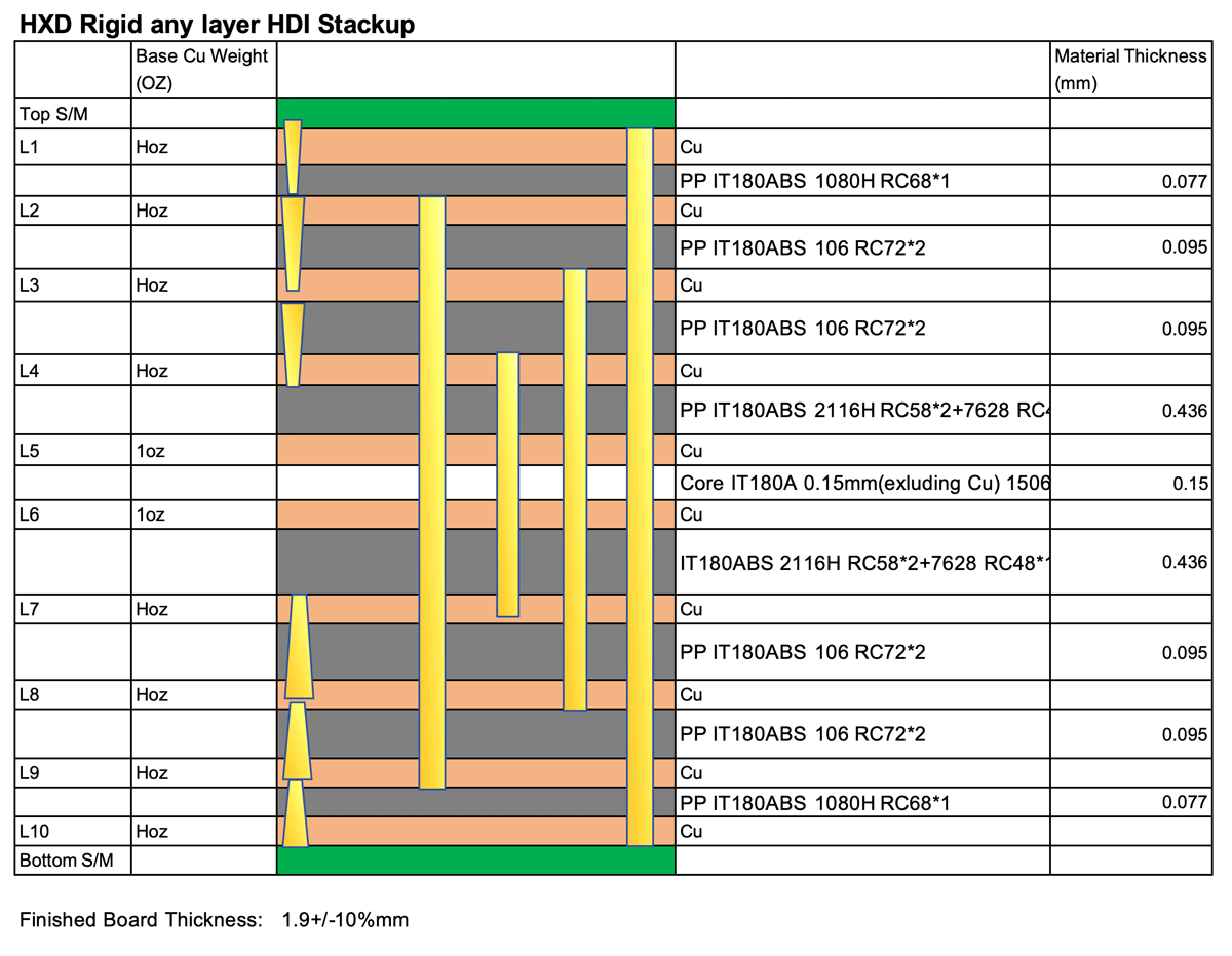
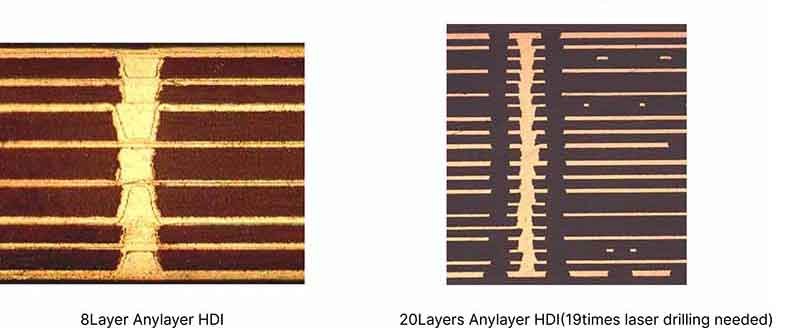
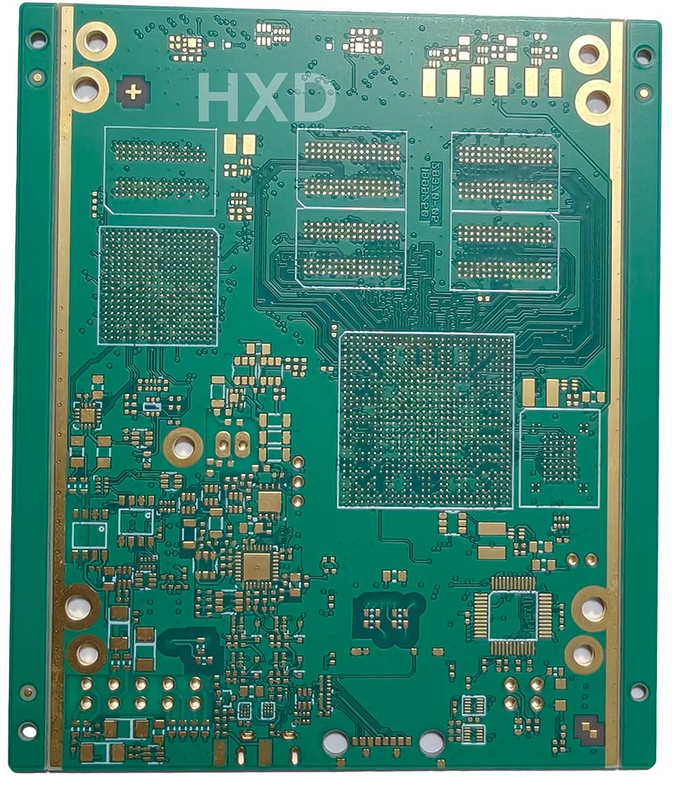
HXD’s HDI PCBs support multilayer structures. With advanced microvia laser drilling and precision lamination technologies, HXD enables high-density routing and reliable interconnections for complex circuit designs.
Support for Advanced Packaging
HXD supports Via-in-Pad processes, enabling direct placement of vias beneath component pads. This helps you design fin-pitch BGAs and high-density components.
Enhanced Stability
HXD supports high-precision stack-up designs. HXD micro-via technology improves board stability during thermal cycling, ensuring your products operate reliably for the long term.
Although the costs of HDI PCB are slightly higher, it effectively reduces total layer count ,reduces board size, and improves signal performance,thereby reducing overall system and assembly costs
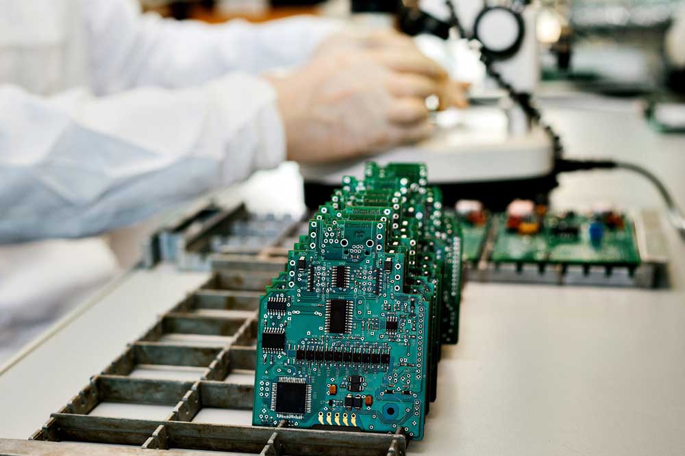
HXD has many years of experience in HDI PCB manufacturing and strict quality control to ensure your designs are realised smoothly from concept to mass production. Whether it’s for consumer electronics, communication devices, or high-end industrial applications, HXD can provide you with high-performance, high-reliability HDI PCB solutions.