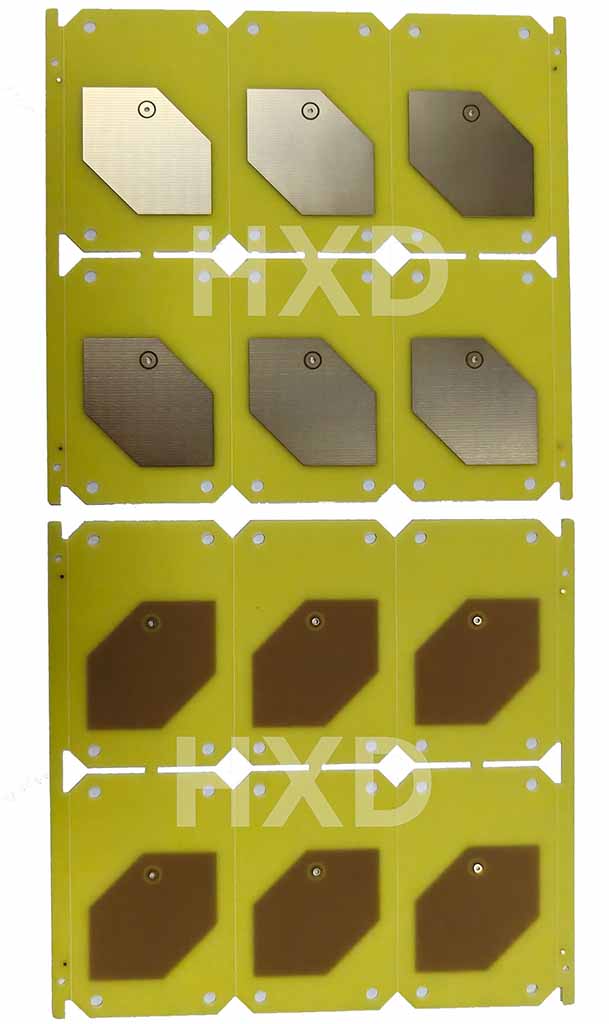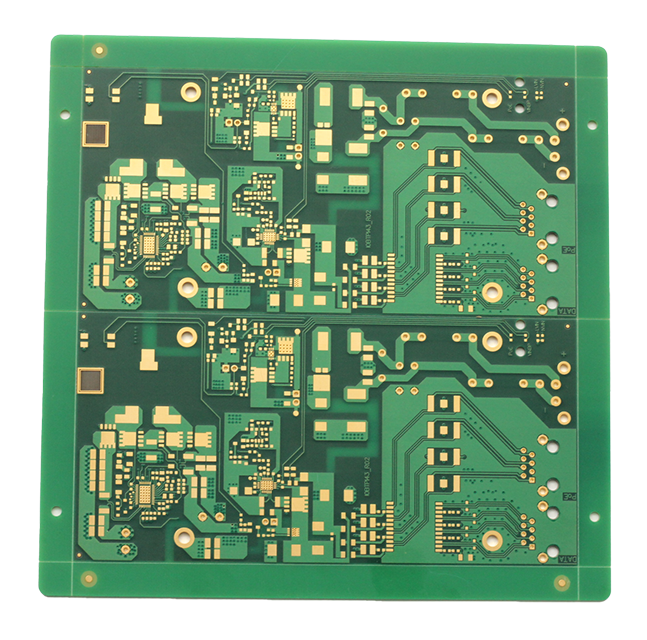


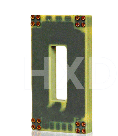
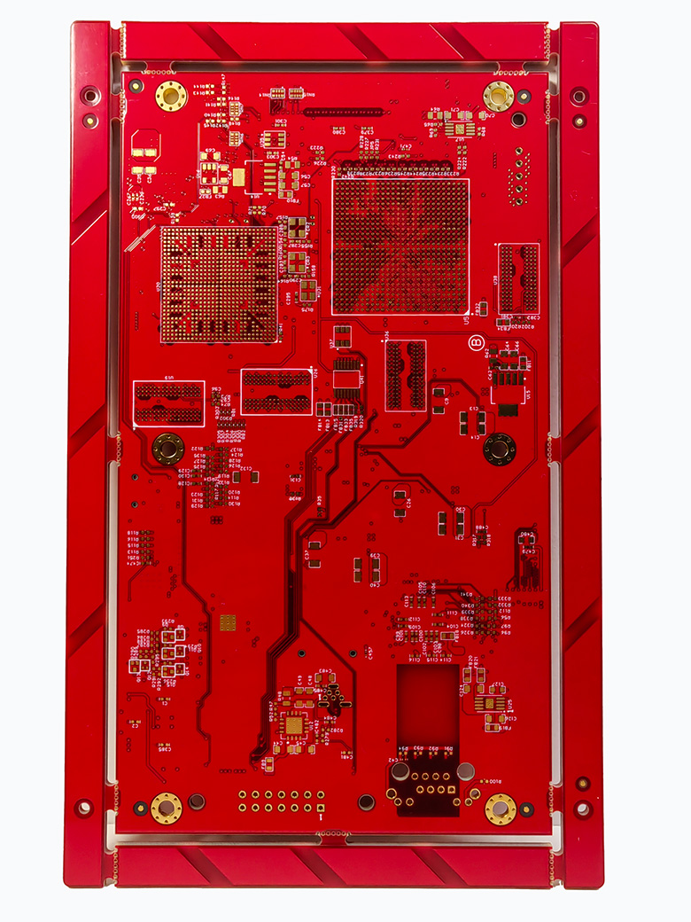
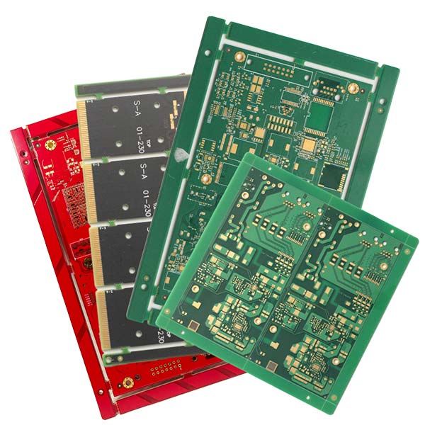
Different Types of Rigid PCB
HXD can supply various rigid PCB types to meet the needs of different electronic applications:
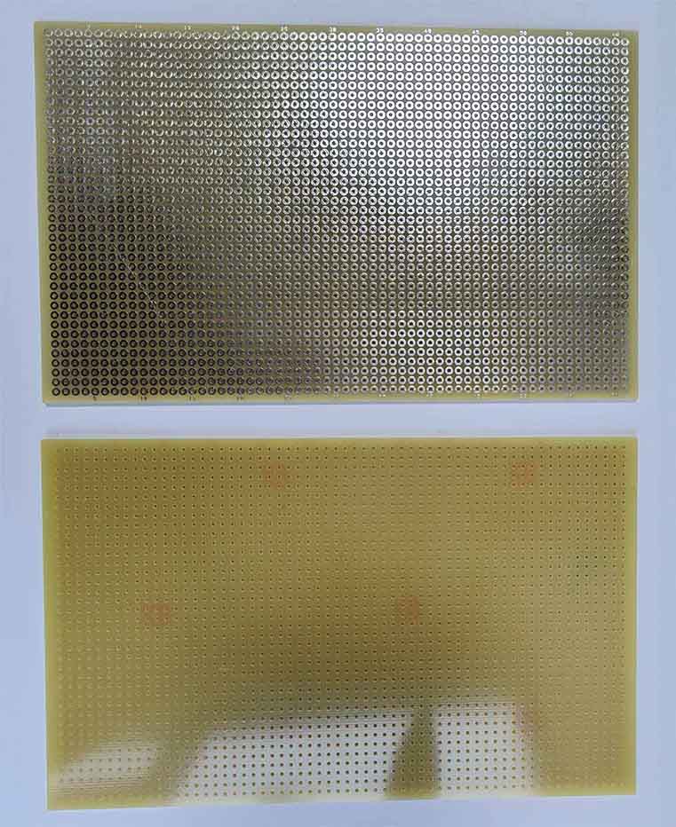
Single-Sided PCB: Conductive traces are only designed on one side of the substrate. It has a simple structure and so the production process is a very mature process. Also the cost is the lowest production cost.
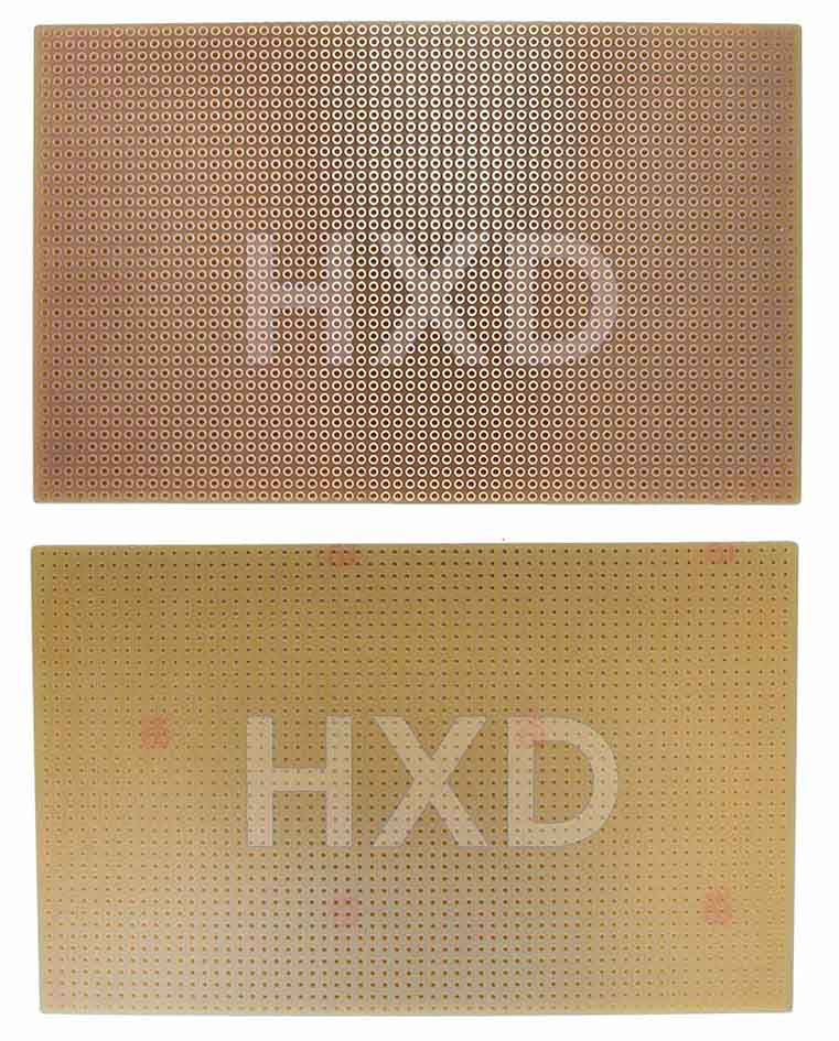
Double-Sided PCB: Conductive circuits are designed on both sides of the substrate. Electrical connections between layers are made through Plated Through Holes (PTH). Compared to single-sided boards, double-sided PCBs offer much higher wiring density. This allows for more components and supports more complex circuit designs.
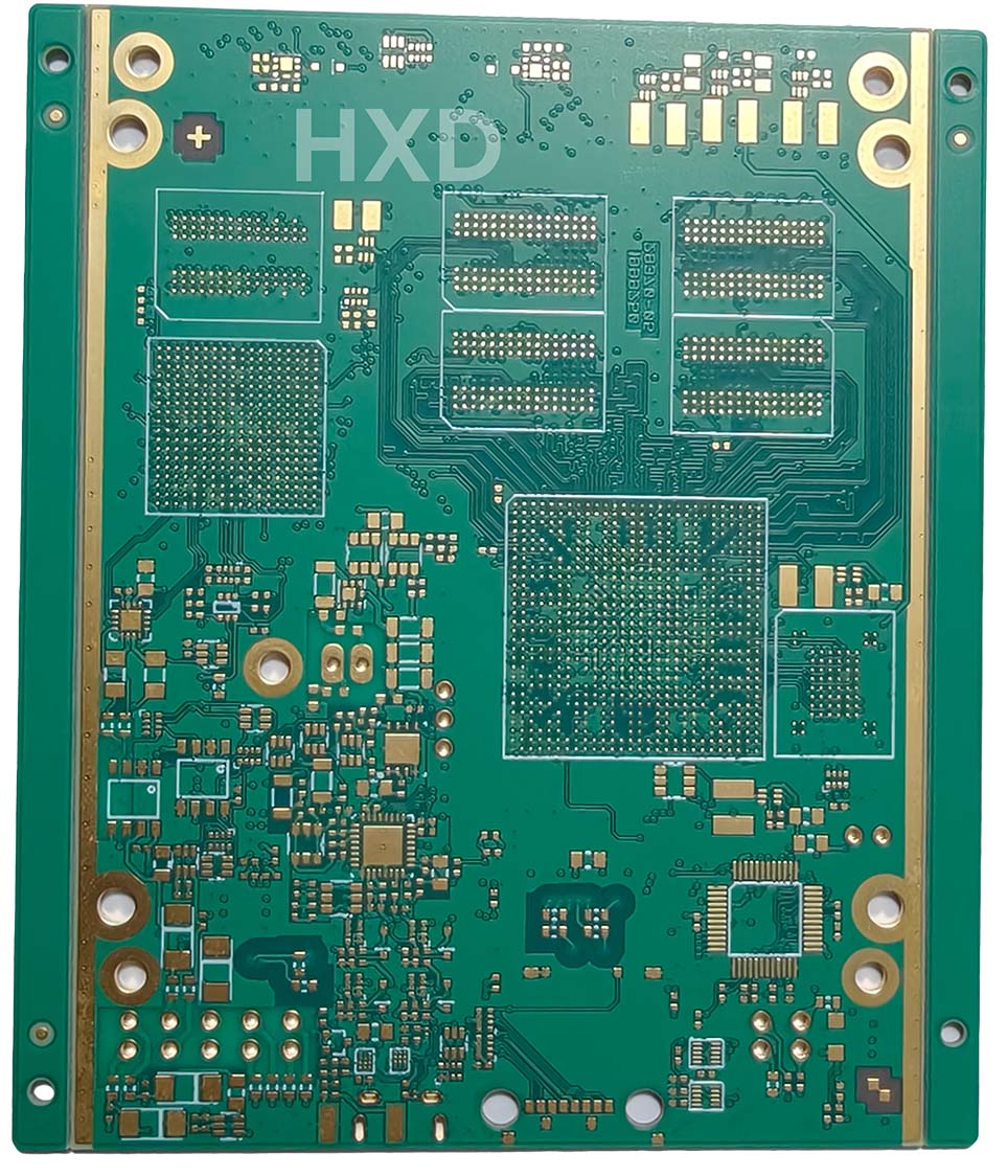
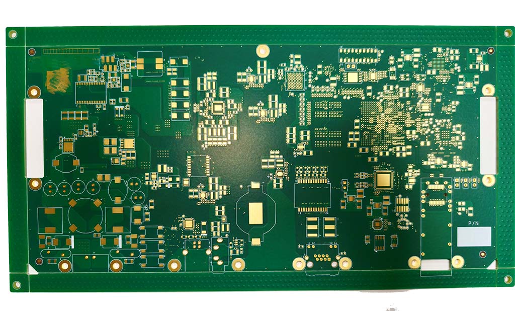
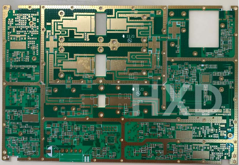
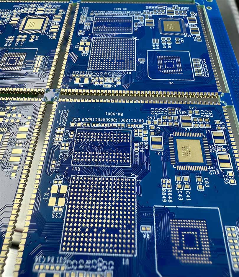
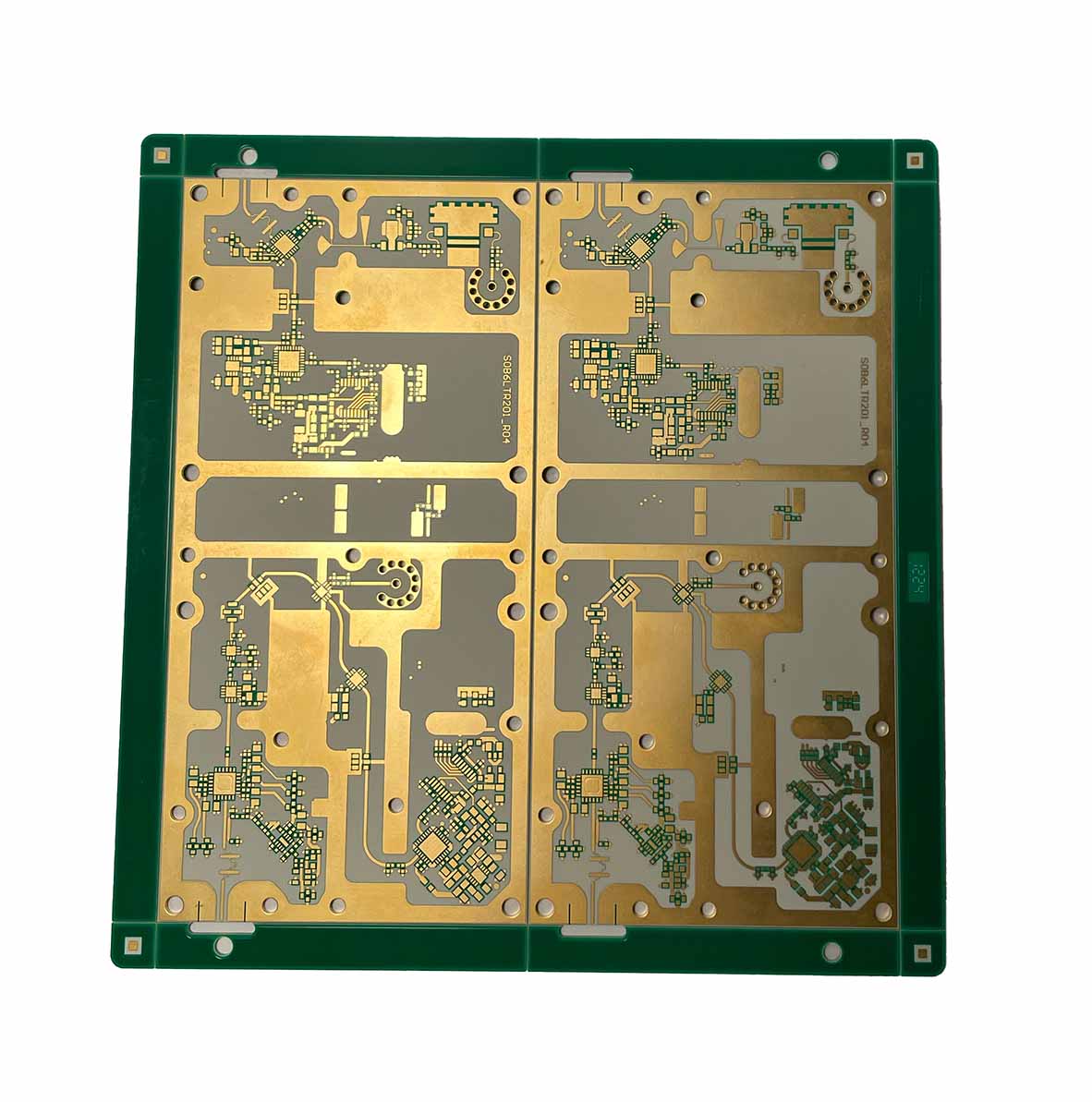
Multilayer PCB: Multilayer PCBs consist of three or more conductive layers separated by insulating materials. These layers are interconnected using advanced via technologies, such as Through-Hole, Blind Vias. Designed for high-performance systems, we provide custom solutions including 4-layer PCBs, 8-layer PCBs, and 10-layer PCBs to meet your specific requirements.