Guidelines for Designing Rigid-Flex PCBs for High-Performance Applications
Introduction
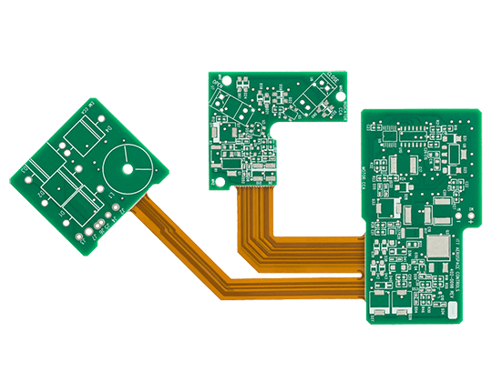
Rigid-Flex PCB is a type of printed circuit board that combines rigid and flex circuit technologies. It offers the mechanical strength of rigid PCBs and the bendable, foldable features of flexible circuits. As electronic products become smaller, lighter, and more powerful, the importance of Rigid-Flex PCBs in modern electronics is growing.
This article explains the structure and design key points of Rigid-Flex PCBs, helping PCB engineers understand design principles and apply them effectively in real projects.
Key Components of Rigid Flex PCBs
A Rigid-Flex PCB consists of several critical parts, each playing a vital role in the board’s function and performance. Understanding these components is essential for successful design and application.
1. Rigid Sections
The rigid areas are similar to standard FR-4 PCBs and are primarily used for mounting electronic components.
- Core: Usually made of FR-4 or High-Tg FR-4 (170+ Tg), providing mechanical support.
- Copper Foil: The conductive paths etched onto the core.
- Soldermask: Applied over the copper surface to prevent soldering shorts and protect the circuits.
2. Flex Sections
The flexible areas allow the board to bend and often run through the rigid regions.
- Flexible Substrate: Typically polyimide (PI), offering excellent heat resistance, insulation, and flexibility.
- Adhesive or Copper Layer: Copper is attached to the PI by lamination or electroplating.
- Coverlay: Acts like a soldermask for flexible circuits. It is usually made of a PI (polyimide) film with an adhesive layer and protects flexible traces from oxidation or breakage during bending.
3. Bonding Materials
These materials bond the rigid and flexible sections into a single unit.
- Prepreg / Adhesive: Standard prepreg is used in rigid areas. In the transition zone between rigid and flex sections, No-Flow or Low-Flow prepreg is used to prevent resin from leaking into the flexible area.
- Flexible Adhesive: Used specifically for laminating flexible layers.
4. Vias
Vias provide electrical connections between different layers.
- Plated Through-Hole (PTH): Drilled through both rigid and flex layers to interconnect all conductive paths.
- Blind & Buried Vias: Used in HDI designs to connect specific layers, saving valuable board space.
5. Specialized Components (Optional)
- EMI Shielding Films: If your design requires EMI/RF protection, you can use special conductive films (such as Tatsuta or APlus) instead of expensive copper layers to keep the board thin and flexible.
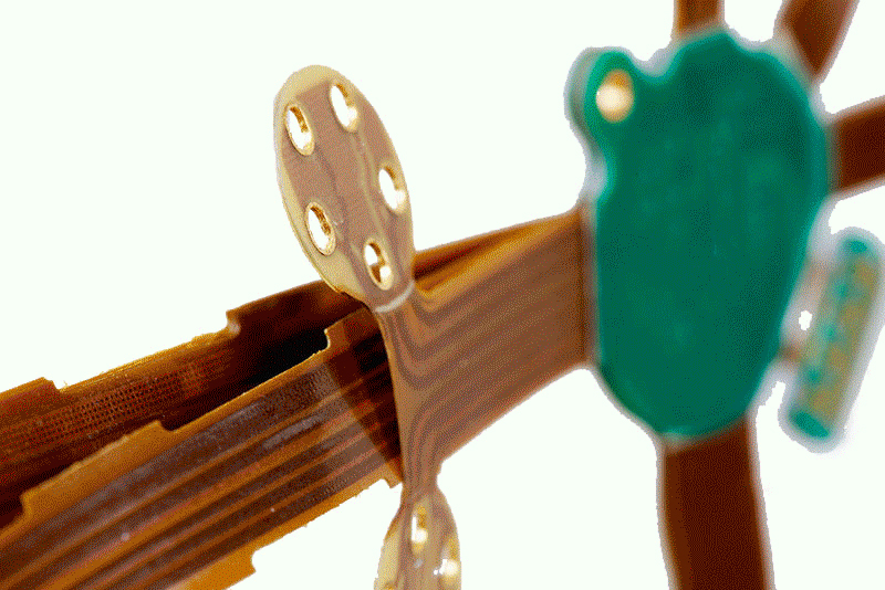
- Integrated Connectors: At the ZIF tail, we can integrate gold finger connections directly on the PCB, eliminating the need for external connectors.
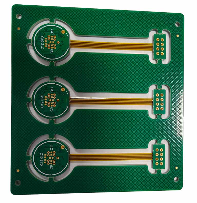
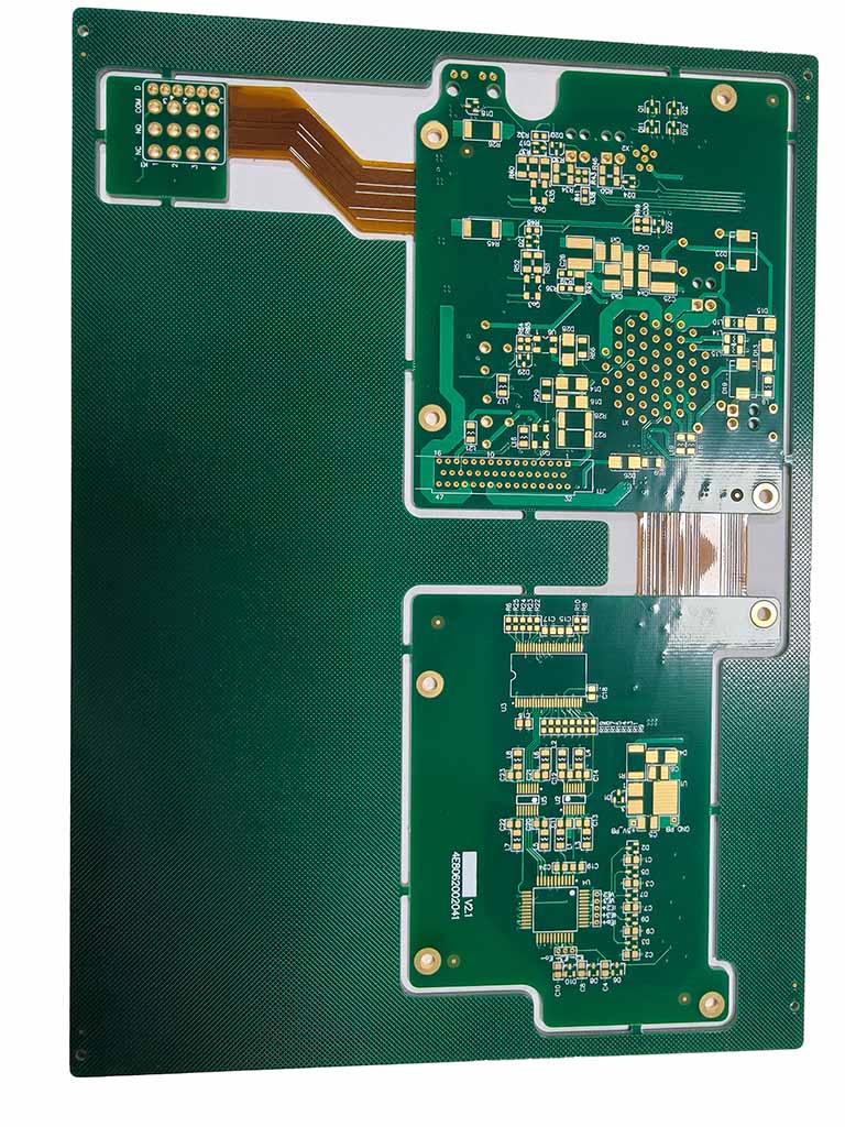
Rigid Flex PCB Stackup
Standard Rigid-Flex PCB Constructions
In most cases, standard rigid-flex PCB designs use a symmetric structure. Whether in the rigid or flex sections, the layer count is typically an even number. This symmetry helps with impedance control and reduces board warping during manufacturing.
Below is a real-world example of an 8-layer rigid-flex PCB.
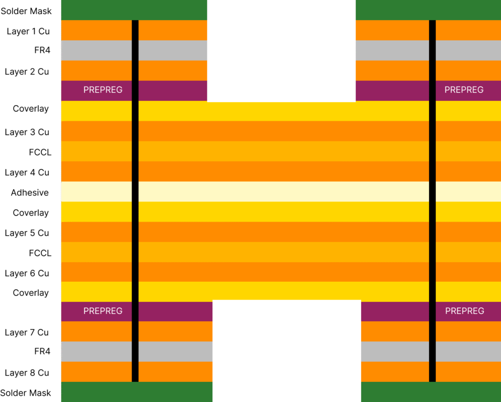
In this example, the board has an 8-layer structure. The number of layers can vary based on your requirements, typically ranging from 4 to 16 layers or more. A key part of this design is that the flexible layers must be located in the center of the overall stackup.
Flexible Circuit with Air Gap Constructions
Air Gap Construction refers to a design where flexible layers are kept as separate layer pairs instead of being fully bonded together with adhesive. This leaves a small air gap between the layers. This structure significantly improves the flexibility and bendability of the flex section, making the circuit more reliable during repeated bending.
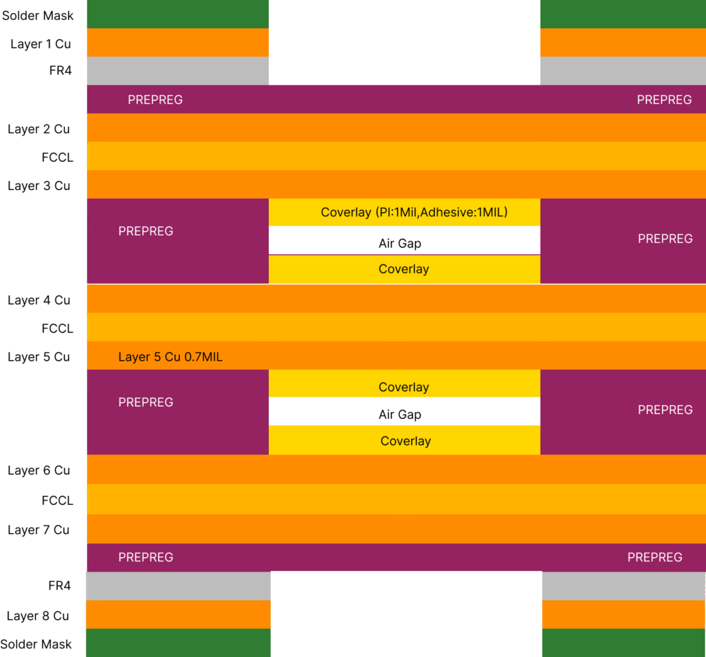
When a flexible circuit has 4 or more layers, air gap construction is often the better manufacturing choice. It makes it easier to meet the requirements of the IPC-2223C design standard. Because of this, it is widely used in multi-layer flex and rigid-flex PCB designs.
Flex Rigid PCB Design Rules
Selecting the Correct Bending Radius
According to IPC-2223 standards, the bending radius is defined as a multiple of the total thickness of the flexible section.
Static Applications (Bend-to-Install): This applies to boards that are bent once during assembly or installation. Depending on the layer count, the recommended bending radius ranges from 6 to 20 times the flex thickness. For very thin 1 or 2-layer designs, IPC-2223 allows for folding (zero-radius bend) under specific guidelines.
Dynamic Applications (Continuous Flex): This applies to boards that must bend repeatedly during device operation. These designs usually require a bending radius of at least 100 times the flex thickness and are typically limited to a maximum of two conductive layers.
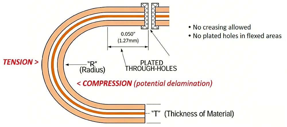
The following reference table is based on IPC standards:
r = Bending Radius
T = Flex Thickness
| Flex Application | Layer Count | Recommended minimum bend radius (r) | Notes |
| Static | 1 | 6xT | |
| Static | 2 | 10xT | The most common industry standards |
| Static | ≥3 | 12xT | |
| Dynamic | 1 | 20xT | Rolled Annealed (RA) copper is required. |
| Dynamic | 2 | 25×T – 50×T |
Flex Routing Rules
When routing in the flexible area, following these basic principles will reduce mechanical stress and improve reliability:
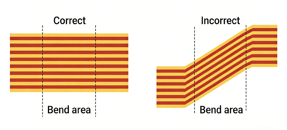
- Trace Direction: Keep traces in a straight line and perpendicular to the bend line whenever possible. This helps distribute stress during bending. Do not stack traces directly on top of each other between layers; instead, use a staggered (zipper) layout to reduce the risk of fracture and increase flexibility.
- Avoid Sharp Angles: Do not use 90° or 45° corners in flex circuits, as sharp angles create stress points. Use rounded (arc) traces to effectively reduce stress on the copper foil.
- Even Distribution: Use narrower trace widths and distribute them evenly across the flex area. In some cases, adding dummy traces can help balance the structure and improve long-term mechanical strength.
Bending Area Design
The bending zone is the most sensitive part of a Rigid-Flex PCB.
- Avoid Vias and Pads: Do not place vias, pads, or plated holes in the bending area. The mechanical stress during folding can cause these metal structures to crack.
- Reinforcement: If pads or connection points are necessary near the bend, use Anchor Reinforcement or Teardrops to strengthen the connection between the pad and the trace. This reduces the risk caused by bending stress.
Via Placement and Transition Zone Clearance
Do not drill vias through coverlay adhesive. Coverlay adhesives used in flexible circuits (such as acrylic or epoxy) have a very high coefficient of thermal expansion (CTE). If a via passes through these adhesive layers, the plated copper may crack due to thermal stress during reflow soldering or temperature changes.
According to IPC-2223, a clearance of at least 0.125 inches is recommended from the rigid-to-flex transition area. For high-density designs, many manufacturers can reduce this distance to 0.050 inches or even 0.040 inches.
Ground Plane Design
In the flexible section, we do not recommend using Solid Copper Planes for grounding. Solid copper makes the PCB stiff and increases the risk of copper cracking during a bend.
Instead, use a Cross-hatched Ground Plane. This mesh-like copper structure provides the necessary grounding while significantly improving flexibility and reliability.
Conclusion
Rigid-flex designs require complex materials and layers. It is critical to sync with your PCB supplier early on based on your specific application. This ensures your design is optimized for manufacturing (DFM) from the start.
HXD offers proven processes and expertise to meet your specific needs. We deliver reliable solutions that help you design and mass-produce high-performance electronics with ease.
Related Rigid-flex Products
10 layer HDI Rigid-flex PCB
Advanced 10-Layer Rigid-Flex Stackup (FR4 + PI) Supports compact medical equipment designs while ensuring long-term bending reliability.
4Layer Rigid-flex PCB
Stable 4-Layer Rigid-Flex Design (FR4 + PI) Combines flexibility and rigidity to support compact layouts and dynamic bending in industrial control applications.
8Layer Rigid-flex PCB with Dupont AP8535R and Arlon 49N
Advanced 8-Layer Rigid-Flex Stackup,hybrid Laminating Expertise
written by
steve ran
Senior Layout Manager