Ultimate Guide to Impedance Control
Impedance control is a vital process in PCB design and manufacturing. It ensures that signals remain stable, noise-free, and strong during transmission.
For PCB designers, improper impedance can lead to signal reflections and increased crosstalk. In some cases, it can cause the entire product to fail functional tests. This guide focuses on real-world needs to help designers master the core rules of impedance control.
What is Impedance Control in PCB?
Impedance is measured in Ohms (Ω), similar to resistance, but they are not the same. While resistance applies to DC (Direct Current), impedance refers to how a circuit opposes AC (Alternating Current) or high-frequency signals.It is a combination of three factors:resistance、apacitance and Inductance.In high-speed and high-frequency PCB design, impedance is a critical electrical parameter that ensures signals move efficiently across the board.
In a circuit, Impedance Control means matching the trace dimensions and location with the PCB material properties. The goal is to ensure that signals remain noise-free and do not lose strength during transmission.
Why Impedance Control Is Important?
You can think of impedance control like controlling road quality when building a highway.If the road suddenly narrows (trace width changes) or the foundation thickness varies (dielectric changes), a car (the signal) traveling at high speeds will bounce or even crash. This causes signal reflection and distortion.
By using impedance control, we ensure the entire “roadway” has consistent specifications. This allows your data to travel smoothly and reach its destination at maximum speed without errors.
Impedance control is essential for several core reasons:
1. Eliminate Signal Reflection
In high-frequency environments, PCB traces act as transmission lines rather than simple wires. If the impedance is inconsistent along the line, the signal will “bounce back” (reflect). This reflection overlaps with the original signal, causing distortion.
Impedance control is the first step toward Signal Integrity. It ensures signals travel smoothly without interference or loss of data.
2. Maximize Power Transfer
According to the Maximum Power Transfer Theorem, signal power flows most efficiently when the impedance of the driver matches the receiver. Without proper matching, high-speed signals will significantly weaken and degrade as they travel across the board.
3.Better System Reliability
Poor impedance control can cause hard-to-an errors, often showing up as timing or synchronization issues. Once the components are soldered, unmanaged impedance is very difficult to analyze.
Sometimes, even replacing the components won’t fix the problem, because the root cause is the trace design, not a faulty part. Proper impedance control makes your system predictable and reliable.
4.Differential Signal Applications
Differential signaling uses a pair of traces (one positive and one negative) to transmit a single signal. To cancel out noise effectively, the width and spacing of these two traces must stay consistent across the entire board. This maintains a specific “differential impedance.”
If the impedance is uneven, the signal will travel at different speeds on each wire. If the positive and negative signals do not reach their destination at the same time, the data becomes distorted, and the system may fail to decode it correctly.
Key Factors That Affect PCB Impedance
PCB impedance is determined by resistance, inductance, and capacitance. The factors that change impedance are grouped into three categories: dimensions, materials, and design structure.
1. Physical and Geometric Factors
These are usually controlled during the manufacturing process, such as etching and plating:
- Trace Width: Inversely proportional to impedance. Narrower traces result in higher impedance.
You can use our online tool to calculate the trace width. - Copper Thickness: Inversely proportional to impedance. Thicker copper results in lower impedance.
- Trace Shape: In reality, the cross-section of a trace is a trapezoid, not a perfect rectangle. This shape is factored into precise impedance calculations.
- Vias and Pads: The thickness of pads and the path signals take through vias can disrupt impedance continuity.
2. Material Properties
- Dielectric Thickness: Proportional to impedance. Thicker dielectric layers (Core or Prepreg) result in higher impedance. The final thickness depends on pressure and resin flow during lamination.
- Dielectric Constant: Inversely proportional to impedance. A higher Dielectric Constant results in lower impedance. This value can change based on the frequency, resin content, and the type of glass fabric used in the board.
3. Structural Factors
- Distance to Reference Plane: The closer a trace is to its reference plane (Ground or Power layer), the stronger the capacitive coupling and the lower the impedance.
- Solder Mask: The presence of solder mask reduces impedance. Typically, one layer of solder mask drops single-ended impedance by about 2Ω and differential impedance by about 8Ω.
- Return Path: Any split or gap in the reference plane breaks the return path. This causes impedance discontinuity and leads to signal reflection.
4.Microstrip&Stripline
In PCB stackup design, Microstrip and Stripline are the two basic structures used for controlled impedance. The main difference is the position of the signal trace relative to the reference planes (Ground or Power layers).
| Feature | Microstrip | Stripline |
| Position | On the outer layers (Top/Bottom). | Inside the inner layers. |
| Reference Planes | Has a reference plane on only one side. | Sandwiched between two reference planes. |
| EMI Shielding | Weak. Signals may spread into the air. | Very Strong. Fields are fully contained. |
| Advantage | Easy to route; no vias needed for surface parts. | Excellent EMI shielding and impedance control. |
| Applications | Standard signals and BGA escape routing. | High-speed digital signals and RF signals. |
| Manufacturing difficulty | Low | High (sensitive to lamination thickness) |
For outer-layer Microstrips, the copper traces are covered by a layer of Solder Mask (green oil).
Since the dielectric constant of solder mask is higher than that of air, the impedance usually drops by 2 to 3Ω after coating. To ensure accuracy, we always pre-adjust the trace width based on the solder mask thickness before production.
If your goal is to maintain the strength and stability of high-speed signals, Stripline is the better choice.However, for simpler routing or standard signals, a Microstrip placed close to the ground plane can also provide reliable impedance control and signal performance.
Impedance Control in PCB Manufacturing
1.Material Selection and Dk Control
Small changes in material properties directly affect impedance.
- DK Stability: Not all FR-4 materials are the same. High-speed designs require materials with stable Dielectric Constants (like Rogers or Panasonic Megtron) across different frequencies.
- Glass Weave Effect: Standard glass cloth has gaps. Because resin and glass fibers have different DK values, impedance can fluctuate. For high-speed boards, we use Spread Glass to ensure a uniform DK.
- Resin Content: The amount of resin in the Prepreg determines the final DK. Manufacturers must carefully match resin levels to the design specs.
2.Dielectric Thickness Tolerance
The distance between the trace and the reference plane is the most sensitive factor for impedance.
- Pressed Thickness: The thickness in your design is a theoretical value. During lamination, resin fills the gaps in the copper, making the layer thinner. Manufacturers must predict the final Pressed Thickness based on the copper density.
- Precision Lamination: We use strict pressure and temperature controls to keep thickness uniform. Standard tolerance is ±10%, while high-precision products require ±5%.
3.Etching Compensation
Chemicals used to etch copper move both vertically and sideways, creating “under-cutting.”
- Trapezoid Effect: The final trace cross-section is a trapezoid, not a perfect rectangle. This shape changes the area through which current flows, affecting impedance.
- CAM Compensation: To fix this, engineers increase the trace width on the production tools. For example, a 5mil trace might be printed as 6mil to account for the copper lost during etching.
4.Lamination Control
Lamination bonds layers together and determines how well they align.
- Layer Alignment: If a signal layer shifts away from its ground plane, the electromagnetic field changes, causing impedance to spike or drop.
- Resin Flow: The pressure must be perfectly balanced. If the resin flows unevenly, the thickness of the dielectric layer will vary across the board.
- Warp Prevention: We ensure the board remains flat. Physical warping can cause small but measurable changes in high-speed signal impedance.
5.Process Capability Limitations
Understanding manufacturing limits is key to a successful design (DFM).
- Width Limits: Most factories have a ±10% width tolerance. For very thin traces (under 3mil), even a tiny etching error can cause a massive change in impedance.
- Plating Variations: Electroplating is not always perfectly even. Differences in copper thickness across the panel can affect precision differential pairs.
- Solder Mask Impact: Solder mask oil lowers impedance by 2 Ω to 5 Ω. Manufacturers must include the mask’s thickness and Dk in their final impedance model.
Impedance Testing and Verification
Even with a perfect design, manufacturing variations can cause signal failure. Strict testing is the only way to ensure the final product works as intended.
TDR (Time Domain Reflectometry) Testing
TDR is the industry-standard technique for measuring PCB impedance. It works like “radar” for circuits.The TDR device sends a fast electrical pulse down the trace. When the pulse hits a spot where the impedance changes, part of the energy reflects back.By measuring the time and strength of these reflections, the equipment calculates the exact impedance at every point along the line. This allows engineers to see exactly where a via, connector, or trace change is causing a problem.
Impedance Test Coupons
Testing directly on the finished board is difficult and can damage the circuit. To solve this, manufacturers use Test Coupons.A coupon is a small test circuit placed on the edge of the production panel. It uses the exact same stack-up, trace width, and spacing as your main board.Because it is made at the same time and on the same panel, the coupon’s impedance accurately represents the quality of your actual PCB.If a coupon fails the test, the manufacturer will inspect the finished boards to see if they meet specifications or need adjustment.
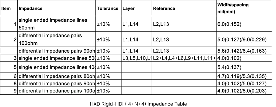
Typical Impedance Tolerance
Because of small variations in materials and manufacturing, impedance is measured within an allowable range (tolerance).
- ±10 Standard Tolerance: This is the general standard for the PCB industry. For a 50Ω requirement, any value between 45Ω and 55Ω is considered a pass.
- ±5 Precision Tolerance: High-performance servers, fiber optics, and military-grade products require tighter control. This requires the manufacturer to have superior control over etching precision and material consistency.
Conclusion
Successful impedance control depends on close collaboration between design and manufacturing.By setting clear impedance targets early, using real-world material data for calculations, and verifying the results with actual measurements, you can significantly reduce design risks. This approach ensures your PCB operates reliably in high-speed and high-frequency applications over the long term.
written by
steve ran
Senior Layout Manager