HXDcircuit

PCB Certifications

HXD Double-sided PCBs

2 Layer 0.4mm Thin PCB with coil track

2 Layer 0.4mm Thin PCB with coil track

Provides excellent solderability and long-term corrosion resistance. Rigid board combined with FR4 stiffener for enhanced mechanical strength.

2Layer Aluminum PCB

2Layer Aluminum PCB

Offers improved routing flexibility and electrical performance compared to standard single-layer MCPCBs—ideal for more complex lighting designs.

2Layer Flex PCB

2Layer Flex PCB

Reliable 2-Layer Construction with ENIG Finish.Ensures stable electrical performance and good solderability.

2Layer Flex PCB with EMC layer

2Layer Flex PCB with EMC layer

Reduces electromagnetic interference, improving signal integrity in sensitive display devices.

2Layer RF board with F4BM255 High-Frequency Material

2Layer RF board with F4BM255 High-Frequency Material

Meets the highest reliability standard for mission-critical electronics—rare for typical 2-layer boards.

2Layer flex with Routed-slot finger

2Layer flex with Routed-slot finger

Highly bendable and lightweight, ideal for compact consumer electronic designs.

2Layer with 0.6mm thin thickness

2Layer with 0.6mm thin thickness

Better Flexibility Than Standard Thickness – Slight bending tolerance makes it suitable for tight assembly structures.

2Layer with 1.2mm FR4 stiffener

2Layer with 1.2mm FR4 stiffener

Provides local reinforcement for connectors or high-stress areas while maintaining overall board flexibility.

Advantages of Double-Sided PCB

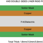
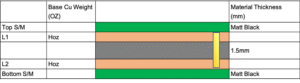
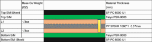
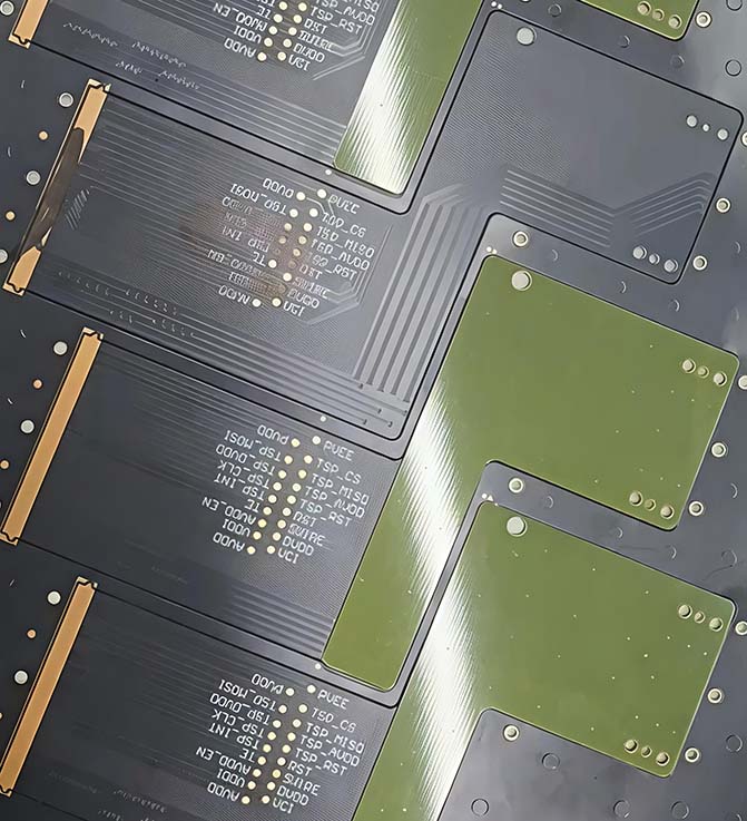
A Double-sided PCB,  also known as a 2-layer PCB, has conductive copper layers on both the top and bottom, with an insulating base material (usually FR-4) in the middle.The two layers are electrically connected through plated through holes (PTHs), enabling reliable signal transmission between layers. Double-sided PCBs offer the following advantages:
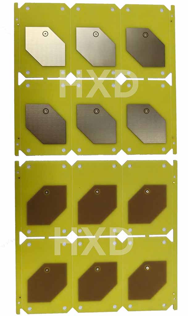
Low Cost: ​​Double-sided PCBs use less material and have a simple manufacturing process. This makes them the most cost-effective choice.They are cost-effective for mass production.

Simple circuits: If your design has few components and signal lines, a single or double-sided layout is enough without extra internal layers.

Fast delivery: Double-sided PCBs have a simpler manufacturing process with fewer steps, resulting in shorter lead times. For 2-Layer Prototypes,HXD can support you 24–48 hours lead time.

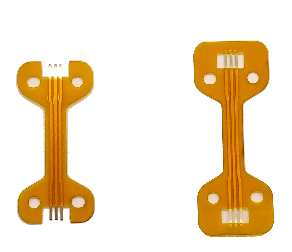
Easy maintenance :Circuit traces are clearly visible on double-sided boards. This makes it much easier to debug, repair, or solder components by hand compared to complex boards.

if your design has very limited space or uses high-speed signals, you should consider a 4-layer or multilayer board. Learn the differences between 2-layer and 4-layer PCBs.

High-Quality Double-Sided PCB Manufacturing with Fast Turnaround

Our double-sided PCBs are manufactured to IPC standards with rigorous AOI and E-test verification, so what arrives at your door is exactly what you designed.

Send Your Gerber Files

HXD Double-sided PCB Manufacturing Capabilities

Features Capabilities
Laminate Materials FR-4, CEM-3, Mid Tg, High Tg, High CTI, Halogen Free. View More Materials
Finished Board Thickness(mm) 16~128 mil (0.4mm – 3.2mm)
Drilling Bit Size 0.2~6.5mm
Copper Foil Thickness 1oz,2oz,3oz,4oz
Impedance control ±10%
Surface Finish HASL,HAL (Pb-free),OSP,Immersion silver,Immersion Tin,Immersion gold(ENIG),
Solder Mask Color Green, Red, Yellow, Blue, White, Black, Matt Green, Matte Black, Purple, None

With 10+ years of factory-direct double-sided PCB production, HXD Circuit delivers consistent quality from prototype to mass production.
Explore our full manufacturing capabilities →

2-Layer PCB Stackup Overview

HXD DOUBLE-SIDED LYAER RIGID PCB STACK-UP

Double-sided PCB is the most basic type of multilayer board.Their structure is simple but reliable:

  • Substrate: Provides mechanical support and insulation, typically FR-4.
  • Copper Layers: Etching creates circuit traces to transmit electrical signals.
  • Solder Mask: Protects copper from oxidation and short circuits; colors include green, blue, red, and black.
  • Silkscreen: Prints component identifiers, logos, and test points.

Below are examples of HXD double-sided rigid PCBs. View more 2-layer flexible PCBs here.

2-Layer PCB Stackup Example 1

2layer-pcb-stackup

Finished Board Thickness 1.6+/-10%
Application Consumer Instrument
Material Shengyi S1000-2
Min. Line W/S 0.1 / 0.1 mm
Surface Finish ENIG
Special Features Different silkscreen colours
IPC Class 3 standard
No minor scratches on solder mask

2-layer-pcb-rigid

2-Layer PCB Stackup Example 2

2-LayerPCB Stack-up

Finished Board Thickness 1.63+/-10%
Application Medical
Material ISOLA 370HR
Min. Line W/S 0.05/ 0.05 mm
Surface Finish ENIG+Hard Gold Plating on Fingers
Special Features Rigid board to be applied with EMI Shielding Layer

2-Layer PCB Stackup Example 3

double-sided-pcb-stackup

Finished Board Thickness 1.2+/-10%
Application Communication
Type PTFE PCB
Material Wangling F4BM255 Tg260
Min. Line W/S 0.2/ 0.2 mm
Surface Finish ENIG
Comment The material lead time for Alon/Teflon is long and the price is very expensive.
Wangling is Chinese brand and can use to replace some of the P/N.

double-sided-pcb-ptfe

FAQ

Is the quality guaranteed for small orders?

Even for a small order of just 5 pieces, we perform 100% E-Test and AOI . This ensures that every board meets your Gerber file requirements.

What is HXD standard lead time?

Prototypes (2-layer): 24–48 hours.
Standard Production: 5–7 working days.
Mass Production: 10–15 working days depending on complexity.

When is it Time to Upgrade from Double-sided to 4+ Layer PCB Designs?

While Double-sided PCB designs are most common, you will most likely need to upgrade in the following circumstances:

  • High Component Density: When you run out of board real estate and have to add a lot of components to finish the routing with only two layers.
  • Complex Packaging: With high-performance microprocessors or BGA packages. The pin density of these devices often exceeds what a 2-layer board can route.
  •  High-Speed Signal Needs: Multi-layer boards are preferred for high-frequency or tightly controlled impedance applications since they often provide dedicated power and ground layers.D


REQUEST A QUOTE

Supported file formats: PDF, DOC, DOCX, TXT, JPG, PNG (Max 2MB)