PCB Stackup Design: A Comprehensive Guide for High-Performance Boards
PCB stackup is the foundation of circuit board design.This article explains common stackup structures, design principles, and manufacturing constraints from an engineering perspective. It helps engineers create reliable stackup plans that work in the real world.
Common PCB Stackup Structures
A standard PCB stackup is usually built by alternating three basic materials:
Copper Layers: These layers carry electricity. They are used for Signal Layers (traces) and Plane Layers (ground or power).
Core: This is the “backbone” of the board. It is a rigid base material with copper foil already bonded to both sides.
Prepreg: This is a fiberglass material coated with resin. During manufacturing, it melts under heat to glue the layers together. Once cooled, it acts as an insulator.
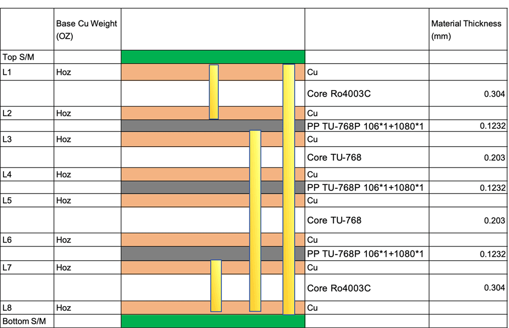
HXD 14-Layer-Rigid-HDI-PCB-Stackup
PCB Stackup Design Principles
PCB design is more than just stacking layers; it must follow the laws of physics and electromagnetics. Here are the core principles of PCB stackup design:
1. The Principle of Symmetry
This is the most basic rule in manufacturing.The PCB structure—including material types, thickness, and copper distribution—must be a mirrored image from the center.
If the stackup is not symmetric, different materials will expand at different rates during reflow soldering. This can cause board warpage or even cracking.
2. The Principle of Tight Coupling
In high-speed designs, signal layers must be placed directly next to a Reference Plane (usually a Ground/GND layer)This helps contain electromagnetic fields and reduce EMI and crosstalk.The dielectric layer (prepreg) between the signal layer and the ground layer should be as thin as possible. A thinner dielectric makes impedance easier to control and more stable.
3. EMI/EMC Suppression
Avoid placing two signal layers directly next to each other. This can cause strong electromagnetic coupling and serious crosstalk.A recommended layer sequence is:Signal – Ground – Power – Signal.This arrangement helps reduce electromagnetic radiation. If you must place two signal layers together, the wiring on the first layer should run horizontally, and the second layer should run vertically. This reduces crosstalk between the two layers.
Impedance Control and Stackup
Impedance control is a key electrical goal in stackup design. To reach specific targets—such as 50Ω Single-Ended or 100Ω Differential impedance—you must precisely adjust the physical parameters of the stackup.Learn more about Impedance Control.
Impact of Material Selection on PCB Stackup
In PCB stackup design, your choice of materials directly determines signal loss, heat management, electrical performance, and total cost.
For designs running at GHz speeds, you must use Low-Dk materials (such as Rogers) to minimize signal distortion and energy loss. Standard FR-4 materials suffer from significantly higher signal loss at these high frequencies.
The insulation layers (Core and Prepreg) help spread heat across the board to prevent “hot spots.” For high-power applications like large LEDs, designers often use Metal Core PCBs (MCPCB) to provide a highly efficient path for heat to escape.
When designing a Hybrid Stackup (mixing different materials), you must choose materials with a similar Coefficient of Thermal Expansion (CTE). If layers expand at different rates when heated, the board will warp, twist, or even delaminate.
FR-4 is the most economical and widely available option.High-performance materials or thick copper foils (for high current) will significantly increase your BOM cost. It is recommended to confirm material availability and real parameters with the manufacturer early in the design stage to balance performance and budget.
PCB Stackup Design Process Recommendations
1. Define Circuit Requirements
Before layout starts, clearly define the board requirements:
- Identify the board type: Confirm whether it is HDI, high-speed digital, RF, flexible, or rigid-flex.
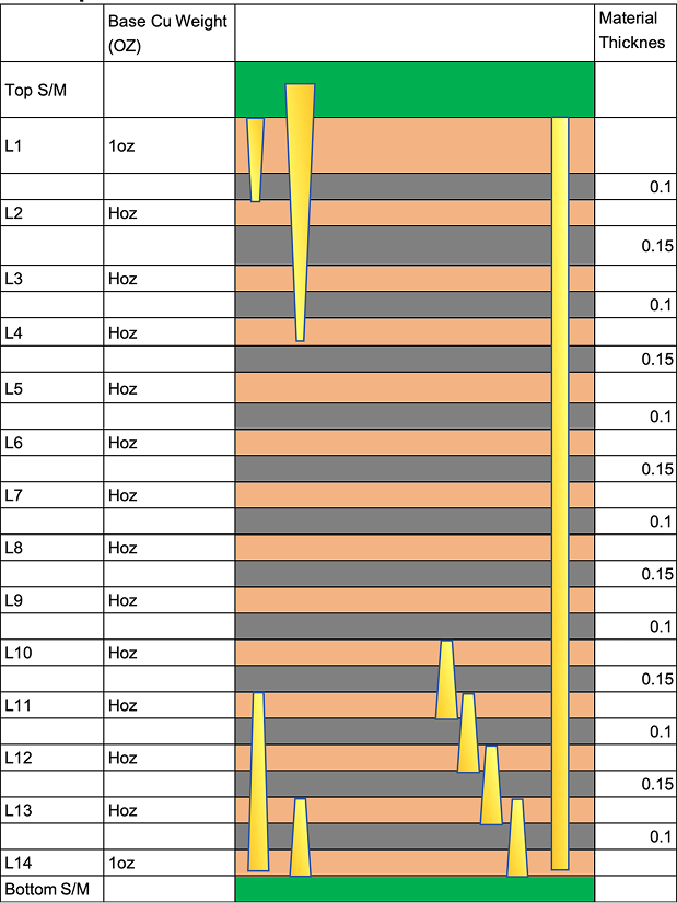
- Estimate layer count: This depends on circuit complexity and signal integrity. For high-speed designs, a 6-layer board is usually the minimum starting point.
- Select Copper Weight: Choose between 0.5 oz to 2 oz (or thicker) based on your current levels and required trace widths.
2. Align with Your Manufacturer (CM) Early
Consult your manufacturer at the start to ensure manufacturability:
- Verify Material Availability: Check if the factory stocks your specific Core or Prepreg. This helps balance cost, lead time, and performance.
- Confirm Manufacturing Tolerances: Ensure the factory can meet your needs for layer alignment (usually ±50μm), total thickness (±10%), and impedance control (±10%).
3. Choose Materials and Lamination Method
- Lamination Method: We strongly recommend Foil Construction. It offers lower costs, better layer alignment, and higher yield than “Cap Construction.”
- Material Properties: For GHz-level applications, use Low-Dk materials to reduce signal loss. For IPC Class 3 standards, ensure dielectric thickness is at least 2.56 mil and consists of at least two prepreg sheets.
4. Layer Arrangement and Electrical Optimization
- Tight Coupling: Place every signal layer next to a solid Ground (GND) plane to provide controlled impedance and the shortest return path.
- Power and Ground Pairs: Keep the distance between power and ground planes as short as possible. This creates “plane capacitance,” which improves the Power Delivery Network (PDN).
- Avoid Adjacent Signal Layers: Use a “Signal-Ground-Power-Signal” sequence to prevent interference (EMI) and crosstalk.
- Maintain Physical Symmetry: Arrange the stackup symmetrically from the center using materials with similar CTE (thermal expansion). This prevents the board from warping during production.
Perfecting Your Manufacturing Documents
Your final design files must include a detailed stackup guide to ensure the factory builds your board correctly. High-quality Fab Notes should cover:
- Layer Details: The total number of layers, their names, and their functions (Signal, Power, Ground, or Mixed).
- Material Specs: The specific material type, thickness, and copper weight for every layer.
- Impedance Requirements: Clear instructions for controlled impedance, including target values (e.g., 50Ω), allowed tolerances (e.g., ±10%), and the specific trace widths and layers they apply to.
- Finished Board Thickness: The final thickness of the completed board and the required tolerance.
Conclusion
PCB stackup determines signal integrity, impedance stability, and EMI performance. A successful high-speed, multilayer PCB depends on three key pillars: a logical layer sequence, the right material selection, and a symmetrical layout.
written by
steve ran
Senior Layout Manager