HXDcircuit

Heavy Copper PCB Manufacturing

From 2oz to 20oz copper — engineered for power, built to last. Get precision-manufactured heavy copper PCBs with fast turnaround and factory-direct pricing.

48 hr

Fastest Prototype

4–20L

Layer Count

2–10 oz

Copper Weight

NO MOQ

Order Any Quantity

led-pcb-copper

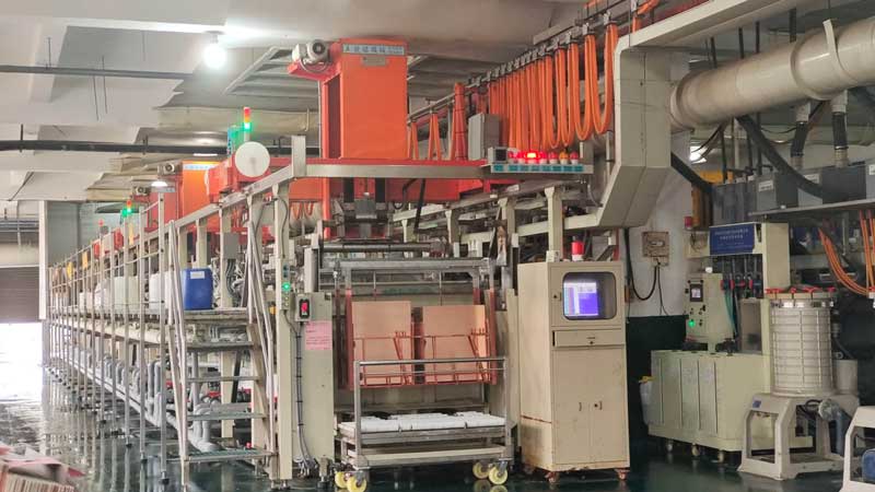
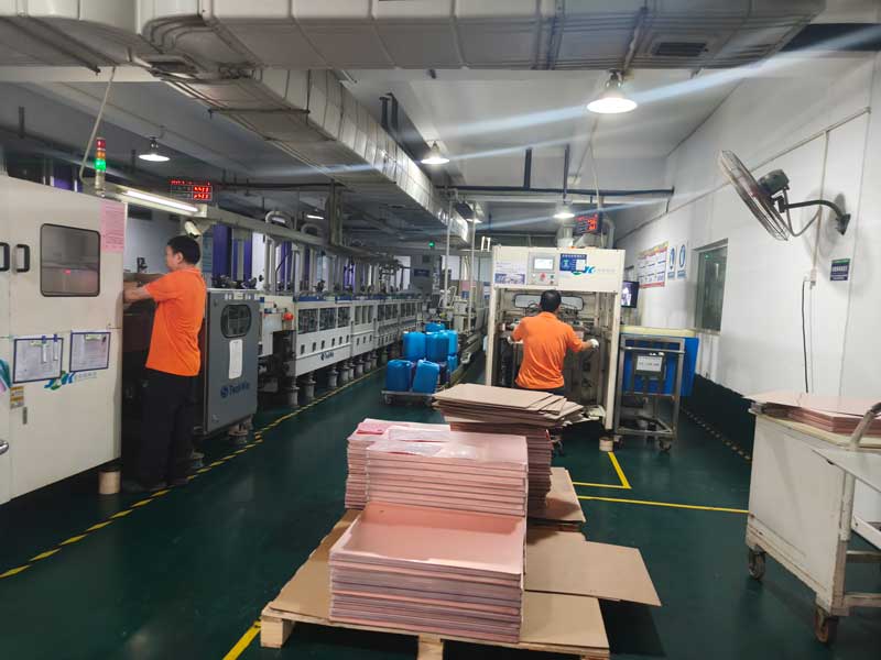
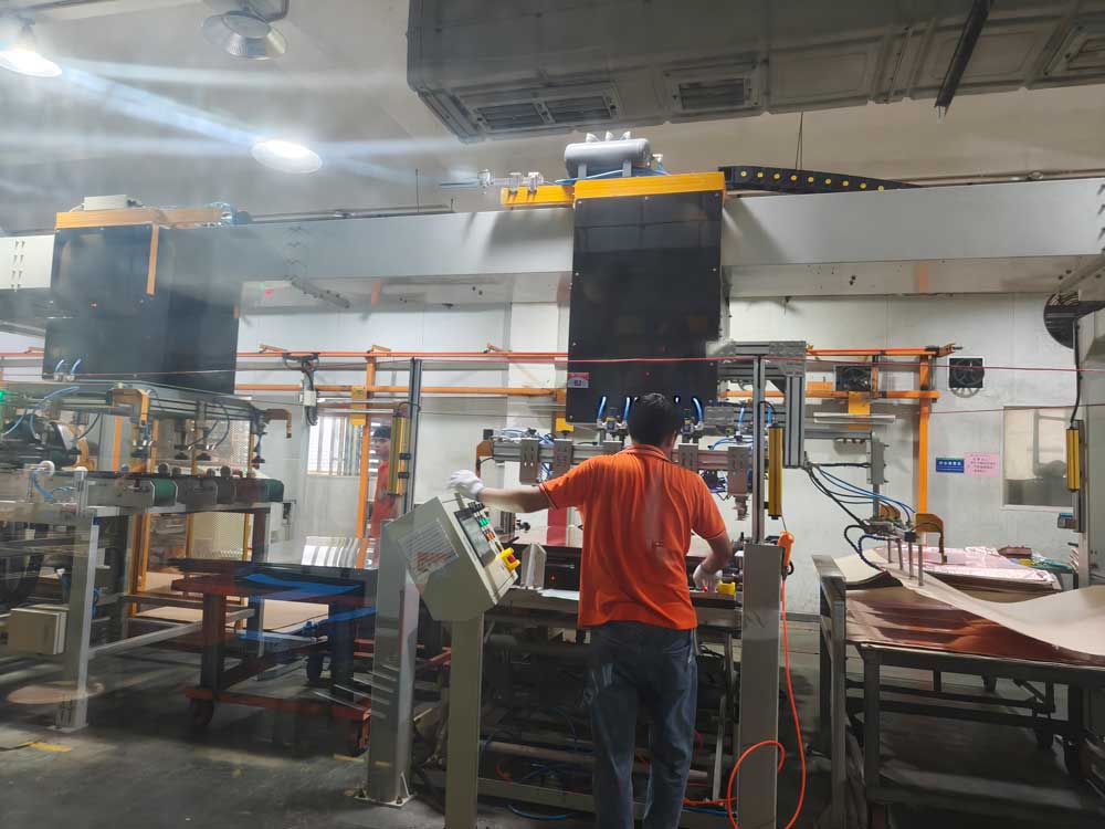
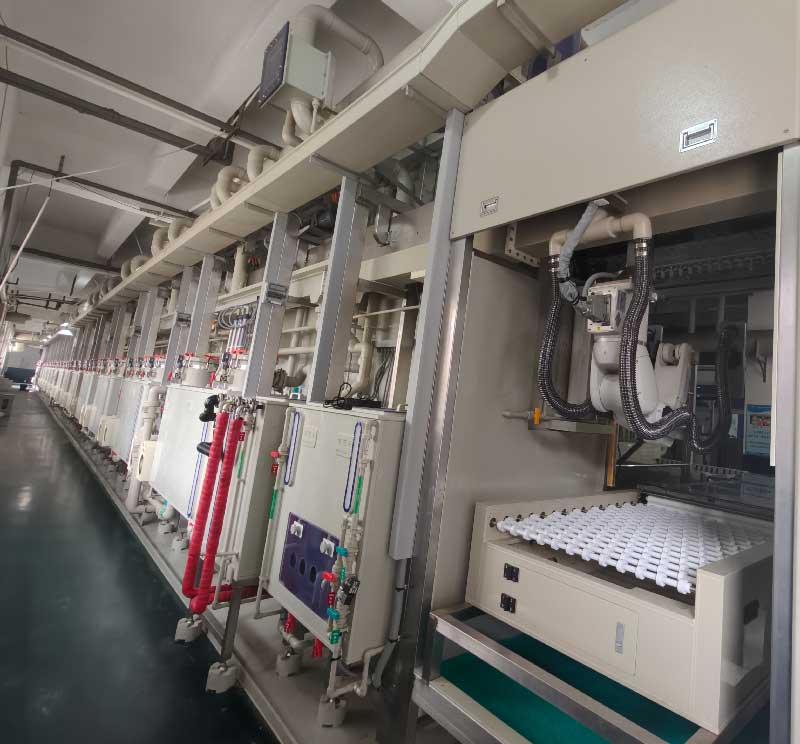
What is Heavy Copper PCB?

A Heavy Copper PCB is a printed circuit board with much thicker copper than a standard PCB. Engineers designed it for high-current and high-power applications. The copper thickness is usually between 3 oz and 14 oz. In comparison, standard PCBs typically have copper thickness from 0.5 oz to 3 oz.

Because the copper is thicker, we need wider traces and spacing to ensure accurate etching and stable production. As a result, the circuit layout is usually simpler than high-density PCBs.

Technical Specs

Heavy Copper PCB Manufacturing Capabilities

Explore our advanced processes, material options, and precision control for reliable heavy copper PCB production.

Items Standard PCB Advanced PCB
Copper Foil Thickness 12μm, 18μm, 35μm, 70μm, 105μm, 140μm (1/3oz – 4oz) 10oz
Max. Panel Size 24 × 28.5″ (622mm × 723mm) 24 × 40″ (622mm × 1000mm)
Laminate Materials FR-4, CEM-3, Mid Tg, High Tg, High CTI, Halogen Free /
Min. Inner Thin Core Thickness 3mil (0.075mm) /
Min. Inner Line Width / Spacing 2.5 / 3.5 mil (0.0635 / 0.089mm) 2.5 / 2.5 mil (0.0635mm)
Min. Outer Line Width / Spacing 3.5 / 3.5 mil (0.089 / 0.089mm) 3.0 / 3.0 mil (0.075 / 0.075mm)
Layer-to-Layer Registration Tolerance ±3mil (±0.075mm) /
Min. Finished Hole Size 0.2mm 0.15mm
Min. Drilling Bit Size 0.2mm /
Max. Drilling Bit Size 6.5mm /
Finished Hole Size Tolerance (PTH) ±0.075mm (±3mil) ±0.05mm (±2mil)
Drilling Precision Tolerance (vs CAD data) ±0.075mm (±3mil) ±0.05mm (±2mil)
PTH Hole Copper Thickness 20–30μm 10–15μm
Max. Aspect Ratio ≤ 10:1 12:1
Min. Solder Mask Opening 0.05mm (2mil) 0.02mm (0.8mil)
Min. Solder Dam 0.076mm (3mil) 0.063mm (2.5mil)
Surface Finish OSP, Peelable Solder Mask, Carbon Ink, HASL (lead free), ENIG, I-Ag, I-Tin OSP, Peelable Solder Mask, Carbon Ink, HASL (lead free), ENIG, I-Ag, I-Tin
OSP Thickness 0.2–0.5μm /
V-Cut Angle 20°, 30°, 45°, 60° /
Min. V-Cut Co-thickness 0.25mm /
Profiling Mode Routing & Punching /
Dimensional Tolerance ±0.10mm (4mil) /
E-Test Voltage 250 ± 5V /
Max. E/T Insulation Resistance 100 MΩ /
Min. E/T Conductive Resistance 20 MΩ /

In addition to heavy copper PCB boards, we also manufacture standard multilayer PCBs for complex and high-performance applications.

HXD’s Advanced Heavy Copper PCB process

Making Heavy Copper PCB is more complicated than making standard PCB. It demands higher technical skills. HXD employs several important processes:

  • Thick copper plating
  • Thick copper etching
  • Substrate lamination
  • High-precision drilling with plated through-holes

These methods help achieve trace accuracy and structural strength in Thick Copper PCBs.
Below are the four core processes :

thick copper pcb Plated-Through-Hole-(PTH)Plating

Thick Copper Plating

Plating quality is critical to the performance of Heavy Copper PCBs. Multiple plating steps are used to achieve copper thickness above 3 oz. This process controls the current to ensure a uniform copper layer. It prevents areas that are too thick or too thin. This high-quality copper plating greatly enhances heat dissipation in high-power applications.
pcb etching

Thick Copper Etching

Compared with standard PCBs, thick copper is harder to etch.
The Copper Etching process strictly controls etch depth to prevent over-etching and line width loss.

pcb-Laminating

Thick Copper Lamination

Plating several times to obtain more than 3oz of copper thickness.This process controls the current to make the copper layer uniform and avoid areas that are too thick or too thin.

Get a Quote

Get a Reliable Heavy Copper PCB Solution

Share your design files and requirements, and our engineers will provide a fast quote with expert support for your high-current applications.

Quote within 2 hours DFM review included IPC-A-600 certified

Key Benefits of Our Heavy Copper PCB

heavy copper PCBs deliver higher current capacity, better heat dissipation, stronger durability, and reliable performance in demanding power applications.

High current carrying capacity

Thick copper safely manages high current without overheating or harming the circuit.

Excellent thermal management

Copper is a good heat conductor. Thicker copper helps move heat away from hot components to the board edges or external heat sinks, reducing hot spots.

Stronger mechanical strength

At connector areas and plated through holes (PTH), thick copper improves structural strength. It better resists shock, vibration, and stress from temperature changes.

Reliable under thermal cycling

It can handle repeated heating and cooling during manufacturing and operation without delamination or trace failure.

Heavy Copper PCB Design Guidelines

Learn the key design rules for heavy copper PCBs, including trace sizing, copper balance, and thermal control to ensure reliable performance.

01

Current and trace width/spacing calculation

Start by sizing the trace width and copper thickness based on the expected maximum current. The industry often uses the IPC-2221A formula to estimate temperature rise, usually keeping it below 30°C above ambient.

02

Trace width and spacing limits

As copper thickness increases, the minimum trace width and spacing must increase. This helps ensure accurate etching. For example, a 4 oz outer layer may need at least 9–13 mil trace/space, while 12 oz may require 20–32 mil.

03

Copper balance

To prevent board warping during manufacturing, the copper distribution should be as symmetrical as possible. Avoid having a large solid copper area on one side and sparse copper on the other.

04

Thermal management design

Put thermal vias under power parts to move heat into inner copper planes or heat sinks.

05

Material selection

Consider the substrate’s Tg (glass transition temperature) and CTE (coefficient of thermal expansion). High current can create thermal stress, which may cause cracks or delamination. Manufacturers commonly use high Tg materials (such as 170°C or higher) or polyimide.

Advanced Equipment for Heavy Copper PCB Manufacturing

HXD has more than 15 years of experience in PCB production. We keep investing in the latest manufacturing and inspection machines. We keep our equipment in great shape, including laser direct imaging and high-precision lamination presses. This ensures your boards are perfect every time.

X-ray Target Drilling

X-ray Target Drilling

PTH Plated Through-Hole-Production Line

PTH Plated Through-Hole-Production LineEtching

pcb-Inner-AOI

Inner AOI

OPE Punching Production Line

OPE Punching Production Line

PCB Chemical Pre-treatment Line

PCB Chemical Pre-treatment Line

Automatic-Dry-Film-Laminator

Automatic Dry Film Laminator

Semi-Auto-Legend-Printing

Semi Auto Legend Printing

VCP-Plating

VCP Plating

15+
Years Manufacturing Experience
50+
Advanced Production Machines
3,000㎡
Clean-Room Production Area
ISO
9001 · UL · IPC Certified

Quality Assurance

Quality Checks for Heavy Copper PCB Production

We manufacture every Heavy Copper PCB through a structured quality process. This ranges from inner layer inspection to final board verification, ensuring your boards perform exactly as designed.

100% Electrical Testing

100% Electrical Testing

Every board is fully tested for open circuits, short circuits, and net continuity before shipment. We use flying probe or fixture-based testing depending on volume, ensuring zero electrical defects reach your assembly line.

100% Automated Optical Inspection

100% Automated Optical Inspection

High-resolution AOI systems scan the inner and outer layers. They find trace defects, missing pads, solder mask misalignment, and other visual issues. This helps catch problems early, saving money.

100% Micro-sectioning TEST

100% Micro-sectioning TEST

We use micro-sectioning to check the inside of the PCB. By cutting a small sample and viewing it under a microscope, we can inspect via plating, layer alignment, and bonding quality. This helps make sure every board is strong and reliable.

100% Final Quality Control (FQC)

100% Final Quality Control (FQC)

Before packaging, each board gets a detailed final inspection. We check dimensions, surface finish, hole quality, silkscreen accuracy, and overall workmanship. This all meets IPC Class 2 or Class 3 standards.

All quality records are traceable and available upon request. We stand behind every board we ship.

Heavy Copper PCB Applications

Automotive and transportation

Automotive and transportation

Used in electric vehicles (EVs) for power converters, battery management systems (BMS), charging stations, and rail systems.

Industrial equipment

Industrial equipment

Common in high-power supplies, inverters, motor drives, welding machines, and power distribution systems.

Military and aerospace

Military and aerospace

Used in radar power systems, weapon control, aircraft actuators, and satellite communication.

Renewable energy

Renewable energy

Used in solar inverters, wind turbine control boards, and energy storage systems.

Medical electronics

Medical electronics

Found in high-end equipment such as MRI systems and laser surgical robots that require high current drive.

Heavy Copper PCB Frequently Asked Questions

How to calculate the current carrying capacity of heavy copper PCB traces?
Engineers often use the IPC-2221A formula to estimate current capacity. They base this on a specific temperature rise. The calculation includes three factors: trace width, copper thickness, and temperature rise. The rise is usually less than 30°C above ambient. Note that inner layer traces can carry only about 50% of the current of outer layer traces.
What is the minimum trace width and spacing for heavy copper PCBs?
When copper thickness increases, the minimum trace width and spacing need to increase too. This change is necessary because of etching limits. For example:

4 oz copper: outer layers usually need at least 9 mil trace/space.

12 oz copper: trace/space may need to reach 20/32 mil.

It is important to check with the manufacturer for exact DFM guidelines for each copper weight.
What substrate materials are commonly used for heavy copper PCBs?
To handle heat from high current, these materials are often used:

High-Tg FR-4: the most common, usually with Tg above 170°C.

Polyimide: suitable for extreme environments up to 250°C.

Metal core boards: such as aluminum or copper base, for excellent heat dissipation.

Ceramic substrates: offer very high thermal conductivity.
Are there special requirements for soldering heavy copper PCBs?
Yes. Thick copper removes heat very quickly, so standard soldering temperatures may not fully melt the solder. Reflow peak temperature is usually higher, around 290°C to 300°C (standard lead-free soldering is about 240°C–270°C).
What is “undercut” in heavy copper PCB manufacturing?
During etching, chemicals remove copper vertically but also attack the sides of traces. This makes the top of the trace narrower than the bottom, forming a “foot” shape. Differential etching and step plating are effective in reducing undercut. These methods also enhance the quality of the sidewalls.
Can different copper thicknesses be used on the same PCB?
Yes. This is often called PowerLink or mixed copper design. It allows different copper weights on the same or different layers (for example, 2 oz for signal control and 20 oz for power lines). This helps meet high current needs while reducing size and cost.
What are the main challenges and cost factors in heavy copper PCB manufacturing?
Heavy copper PCBs cost more than standard PCBs due to:

Material usage: large amounts of expensive copper foil.

Process complexity: longer plating time and multiple solder mask steps (sometimes using spray coating for even coverage).

Drilling difficulty: thick copper increases tool wear and makes chip removal harder.

REQUEST A QUOTE

Supported file formats: PDF, DOC, DOCX, TXT, JPG, PNG (Max 2MB)