24hr
Prototype Turnaround
1oz+
Copper Weight
0.075mm
Min Trace / Space
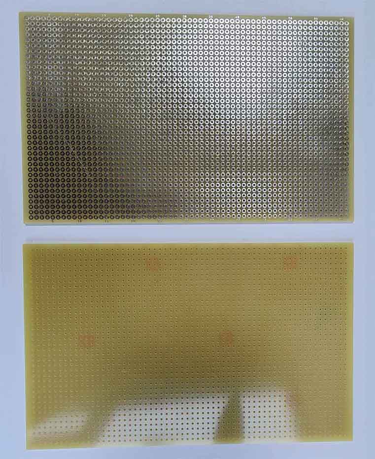
Single Sided PCB Products
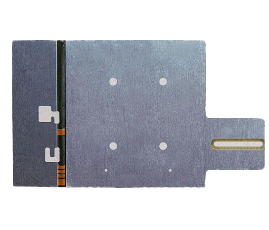
1Layer Aluminum PCB+PI
Aluminum + PI Hybrid Structure Combines high thermal conductivity with flexible PI, enabling creative designs and flexible interconnections not possible with standard MCPCBs.
1Layer Copper based PCB with Pillar Technology
Copper Core for Extreme Heat Dissipation Designed for high-power lighting applications, offering exceptional thermal conductivity up to 400 W/m·K, far beyond standard aluminum MCPCBs.
1Layer with HASL LF
FR4 Material with HASL LF– Cost-effective and ideal for beginner projects, quick prototyping, training, and educational use. HASL LF has excellent solderability for repeated testing and manual solder experiments.
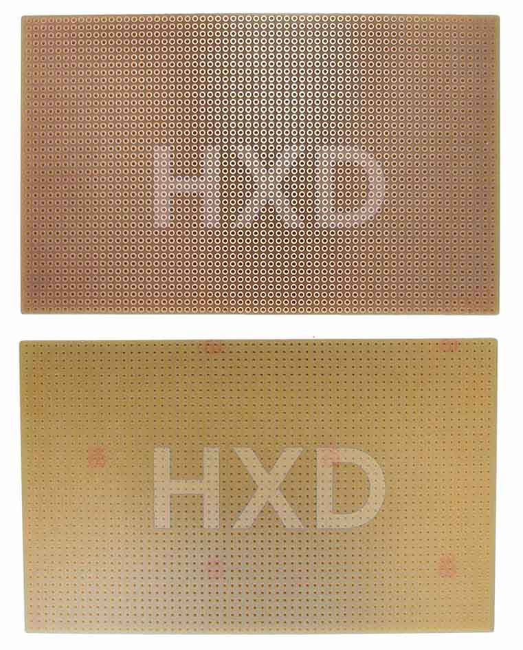
1Layer with KB FR1
FR1 Material with OSP – Cost-effective and ideal for beginner projects, quick prototyping, training, and educational use.
Technical Specs
Single Sided PCB Manufacturing Capabilities
Full spec sheet for standard production runs.
| Parameter | Standard | Advanced |
|---|---|---|
| Layer Count | 1 Layer | 1 Layer (thick copper / special material) |
| Base Material | FR4, CEM-1, CEM-3 | Aluminum,Flex, Copper-based |
| Min Trace / Space | 0.15 / 0.15 mm | 0.075 / 0.075 mm |
| Copper Weight | 1 oz (35 µm) | 2–12 oz (thick copper) |
| Board Thickness | 0.4 – 3.2 mm | 0.2 – 5.0 mm (custom) |
| Min Drill Hole | 0.3 mm | 0.2 mm |
| Max Board Size | 500 × 600 mm | 600 × 1500 mm (custom) |
| Surface Finish | HASL, LF HASL, OSP | ENIG, Immersion Silver / Tin, Hard Gold |
| Solder Mask Color | Green, Black, Blue, Red, White, Yellow | Matte, custom Pantone |
| Tolerance (outline) | ±0.2 mm | ±0.1 mm (CNC routing) |
| Quality Standard | IPC Class II | IPC Class III (on request) |
| Min Order Quantity | NO MOQ | MOV for production |
| Prototype Lead Time | 24 hours | 12 hours (rush, surcharge applies) |
Advanced specs subject to DFM review. Contact engineering for out-of-spec requirements.
Ready to Order Your Single Sided PCB Board?
Upload your Gerber files now and receive an instant price.Lowest cost of PCB board single side — prototype in 24 hours, with IPC-certified quality guaranteed.
Definition
What Is a Single Sided PCB?
A Single-Sided PCB is the most simplest type of PCB. Its key feature is that it has only one layer of conductive material (usually copper) on one side of the substrate, while electronic components are typically mounted on the other side.
Because there is only one conductive layer, the traces cannot cross or overlap. Single-sided PCBs are best suited for low-density circuits with a small number of components and simple routing. They are widely used in consumer electronics, home appliances, and basic industrial control applications.
Single-Sided PCB — Cross-Section Structure
PCB Comparison
Single-Sided vs. Double-Sided vs. Multilayer PCBs
Understanding the structural differences between each board type helps you make the right choice for your design — balancing cost, routing complexity, and electrical performance.
| Feature |
Single-Sided1 copper layer
|
Double-Sided2 copper layers
|
Multilayer4 – 32+ layers
|
|---|---|---|---|
| Layer Count | 1 (top only) | 2 (top + bottom) | 4 – 32+ layers |
| Manufacturing Cost | ★ Lowest | Medium | Highest |
| Circuit Density | Low | Medium | High — BGA / HDI capable |
| Signal Integrity | Basic | Good (via stitching) | Excellent (GND/PWR planes) |
| EMI Shielding | Limited | Moderate | Strong (inner planes) |
| Both-Side Assembly | ✕ | ✓ | ✓ |
| Controlled Impedance | ✕ | Limited | ✓ |
| Prototype Lead Time | ★ 24 hrs | 24 – 48 hrs | 24 hrs (4L) – 7+ days (16L+) |
| Design Complexity | ★ Simple | Moderate | Complex (stackup, SI, via strategy) |
| Typical Applications | LED, power supply, home appliances | Industrial control, IoT, consumer electronics | 5G, servers, medical, ADAS |
| Frequency Support | DC – ~100 MHz | Up to ~500 MHz | Up to 77 GHz+ (Rogers material) |
Why Single-Sided
Key Advantages of Single-Sided PCBs
For many high-volume, cost-sensitive products, single-sided PCBs remain the most practical choice. Here's why engineers and manufacturers continue to rely on them.
Cost-Effectiveness
Single-sided PCBs have a simple design and only one layer, which enables short production cycles in mass production. They are the most cost-effective option among all PCB types
Simplicity in Design and Manufacturing
The single-layer structure does not require complex stackup design, via impedance matching, or layer alignment. The manufacturing process is also simpler — no lamination and no inner-layer inspection are needed. This simplicity shortens engineering review cycles and also reduces the difficulty of new product development.
Easier Testing and Repair
All traces and components of a single-sided PCB are located on one surface, making the board easy to test. ICT fixtures are simpler and more cost-effective. Field repair and rework are also more convenient — technicians can visually inspect solder joints, trace continuity, and component placement directly.
Ideal for Simple Applications
Many everyday products, such as LED lighting strips, switching power supplies, remote controls, and battery chargers, have relatively low electrical complexity and do not require multilayer PCB design. Single-sided PCBs can meet these application needs well, providing sufficient current capacity, thermal performance, and signal quality while avoiding the extra cost caused by unnecessary additional layers.
Faster Production Times
Single-sided PCBs do not require inner-layer bonding, multiple lamination cycles, or blind and buried via drilling, allowing them to move through the production line faster. Prototypes can be completed in as fast as 24 hours, and mass production typically takes only a few days instead of weeks.
Design Guide
PCB Design Considerations for Single-Layer Boards
A well-planned single-layer layout avoids the most common pitfalls — trace crossing, thermal hotspots, and EMI noise — before the board ever reaches fabrication. Follow these guidelines to get it right the first time.
Keep Traces on One Side — Use Jumper Wires Sparingly
The golden rule of single-layer routing: all copper traces must live on the component side. When traces genuinely must cross, use a through-hole jumper wire (zero-ohm resistor) as a single bridge — but treat every jumper as a cost and reliability penalty. Restructure the schematic block order or rearrange component placement to eliminate crossings wherever possible before falling back on jumpers.
Plan Component Placement to Minimise Trace Length
Group functionally related components together and place them in signal-flow order (input → processing → output). Short traces reduce resistance, stray inductance, and susceptibility to interference. Power components (rectifiers, regulators, MOSFETs) should sit close to their bulk capacitors, and high-current paths should run in straight lines to avoid unnecessary bends that add length.
Size Traces for Current — Don't Default to Minimum Width
Single-sided boards carry all current in one layer, so trace width directly determines temperature rise. Use IPC-2221 tables or an online trace-width calculator for every power rail. As a quick reference: 1 A → 0.5 mm, 2 A → 1 mm, 5 A → 2.5 mm (1 oz copper, 10 °C rise). Ground and power fills are preferred over thin traces for high-current paths.
Use Copper Pours for Ground and Thermal Relief
A solid ground pour on the component layer serves double duty: it lowers ground impedance (reducing noise) and acts as a heat spreader for power components. Connect all ground pads with thermal-relief spokes to prevent cold solder joints during wave or reflow soldering. Leave at least 0.3 mm clearance between the pour and non-ground pads to prevent solder bridging and short circuits during assembly.
Respect Minimum Clearance and Annular Ring Rules
For standard single-sided manufacturing, keep trace-to-trace clearance ≥ 0.2 mm and pad-to-trace clearance ≥ 0.3 mm. Through-hole pads should have a minimum annular ring of 0.15 mm after drilling. Tight clearances increase the risk of shorts during etching and solder bridging during assembly. When in doubt, apply HXD’s standard DFM rules before submitting Gerber files — our engineers review every order before fabrication.
Add Test Points and Fiducial Marks for Mass Production
Place exposed test pads (≥ 1 mm diameter, no solder mask) on all key nets — power rails, output voltages, and signal lines — to simplify ICT and functional testing. Add at least two fiducial marks at diagonally opposite corners of the board for SMT pick-and-place alignment. These small additions cost nothing in fabrication but can save significant time and rework cost on the assembly line.
Single-Layer DFM Checklist
- ✓ All traces on component side only
- ✓ Trace-to-trace clearance ≥ 0.2 mm
- ✓ Minimum trace width ≥ 0.15 mm
- ✓ Annular ring ≥ 0.15 mm
- ✓ Ground pour with thermal relief
- ✓ Test points on all key nets
- ✓ ≥ 2 fiducial marks for SMT
- ✓ Jumper wires ≤ 2 per board
Common Design Mistakes
- ✕ Too many jumper wires (assembly cost rises)
- ✕ Undersized power traces causing overheating
- ✕ Copper pour without thermal relief spokes
- ✕ Missing test points — forces manual probing
- ✕ Tight clearances near high-voltage traces
Need a DFM Review?
Our engineers check your Gerber files for free before production starts.
FAQ
Frequently Asked Questions
Common questions about single sided PCB board ordering, pricing, and production.