24-Hour Prototype Turnaround
Standard 4-layer PCB protos shipped in 24 hours. 6–8 layer in 72 hours. Our dedicated fast-track line never compromises on quality for speed.
24 hr
Fastest Prototype
4–20L
Layer Count
±5%
Impedance Tolerance
0.075mm
Min Trace / Space
Reliable Supply of ISOLA 370HR (Tg170),Industrial-Grade 12-Layer Stack-Up,High-Precision Conductive Performance
12-layer stackup with multiple HDI build-up (L1-2, L11-12) enables high-density routing, compact layouts, and advanced miniaturized designs.
Designed for complex, high-speed broadcasting systems requiring multi-layer signal integrity and stable performance.
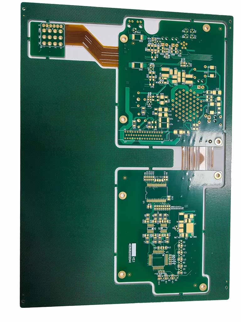
Advanced 8-Layer Rigid-Flex Stackup,hybrid Laminating Expertise
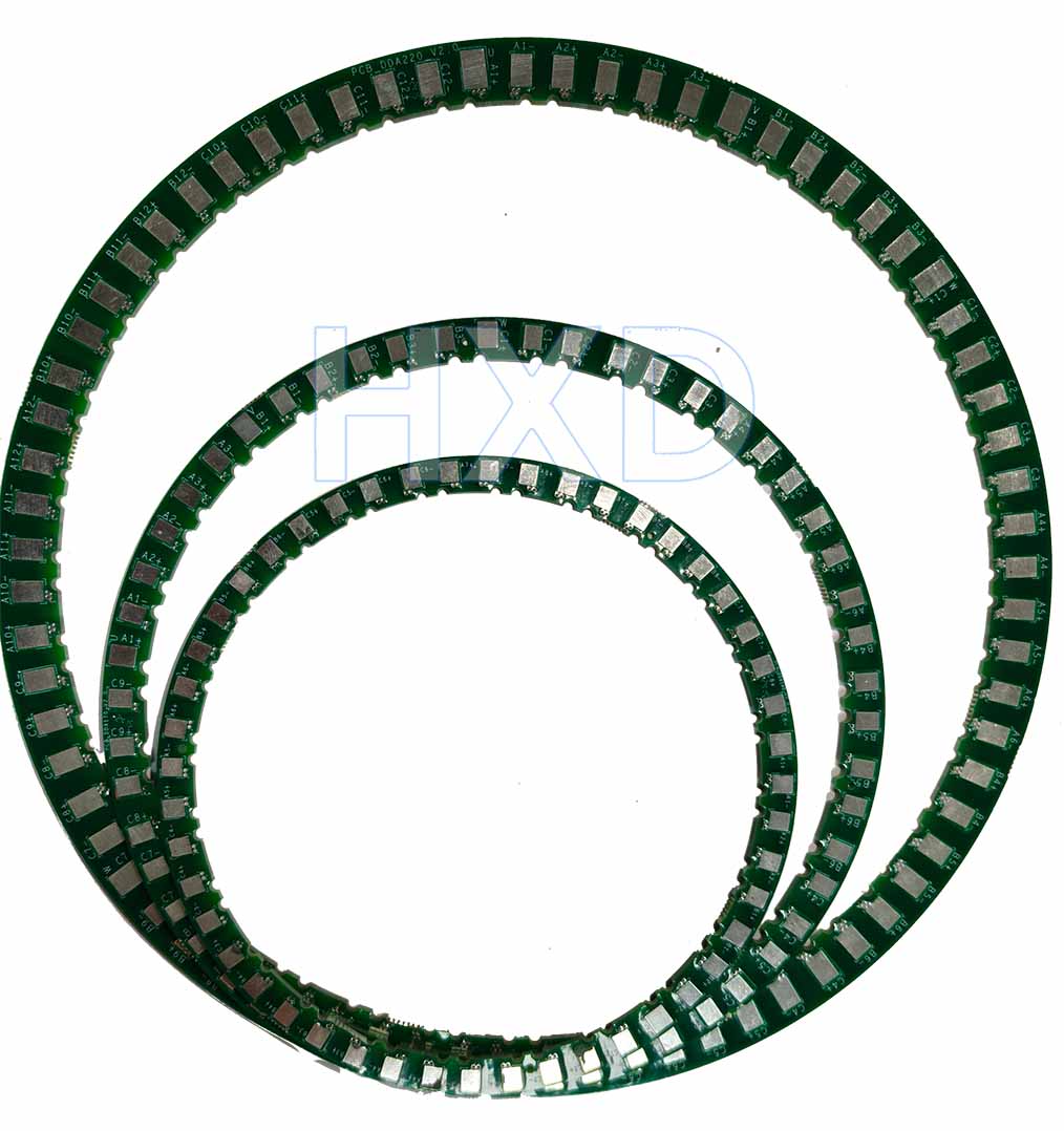
Our 6-layer round PCB combines a complex circular shape with high-density 4/4mil track
Our hard gold fingers are plated with a thick 40μ of gold, specifically designed to withstand thousands of mating cycles without wear, ensuring long-term reliability.
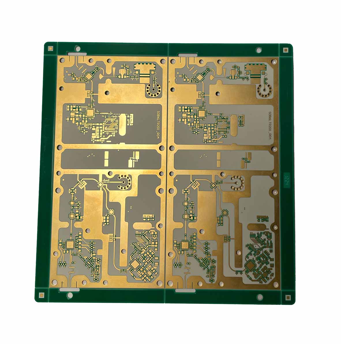
Hybrid Material: FR4 Tg170 + Rogers 4350,4-Layer Rigid Structure for Broadcasting Applications,High-Precision PCB Capability
Edge-plated half holes enable module plug-in, board-to-board connection, and compact mechanical integration.
HXD Multilayer Experience
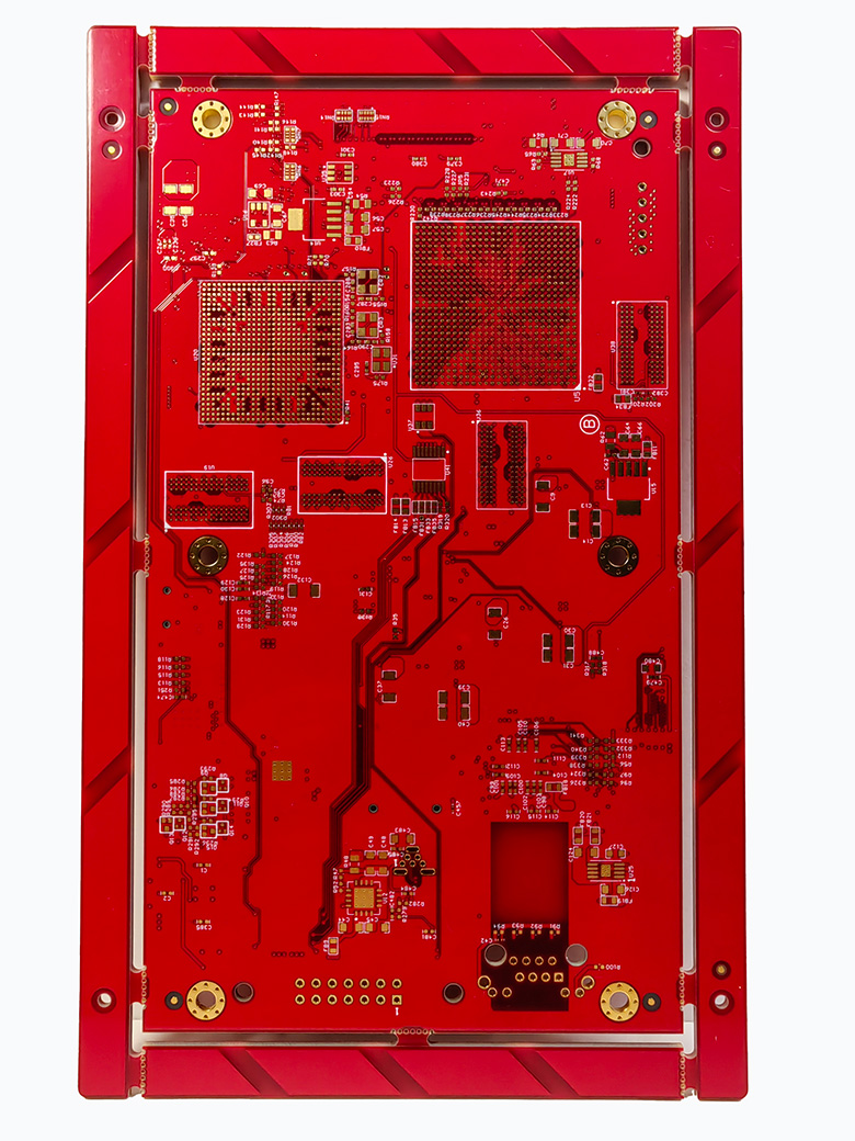
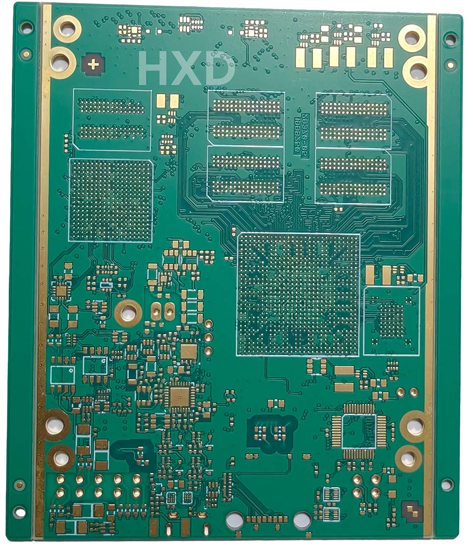
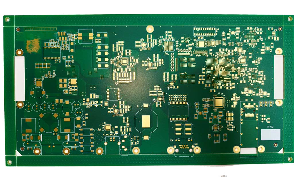
With years of experience in multilayer PCB manufacturing, HXD offers full-stack production capabilities for 4, 6, 8, 10, 12, and 14-layer boards. Our advanced facilities and strict quality control ensure every board meets your exact requirements — from prototype to mass production. Trusted by engineers and procurement teams worldwide, HXD is your reliable partner for complex multilayer PCB projects.
Browse by Layer Count
4-Layer PCb
Consmer
8-Layer PCb
5G· Medical
10-Layer PCb
Server· GPU
12-Layer PCb
HDI · Automotive · High-Speed
Need 16, 20 layers or more?
Our engineers handle complex stackups on request
Technical Specs
Full spec sheet for standard production. Need tighter tolerances? Contact our engineering team for a custom process review.
| Items | Standard PCB | Advanced PCB |
|---|---|---|
| Layers Count | 2–16 layers | 18–20 layers & HDI products |
| Finished Board Thickness | 16~128 mil (0.4mm – 3.2mm) | / |
| Laminate Materials | FR-4, CEM-3, Mid Tg, High Tg, High CTI, Halogen Free | / |
| Finished Board Thickness Tolerance | < 1.0mm ±0.10mm (±4mil) 1.0~1.6mm ±0.15mm (±6mil) | < 1.0mm ±0.075mm (±3mil) 1.0~1.6mm ±0.10mm (±4mil) |
| Min. Inner Line Width / Spacing | 2.5 / 3.5 mil (0.0635 / 0.089mm) | 2.5 / 2.5 mil (0.0635mm) |
| Min. Outer Line Width / Spacing | 3.5 / 3.5 mil (0.089 / 0.089mm) | 3.0 / 3.0 mil (0.075 / 0.075mm) |
| Copper Foil Thickness | 12μm, 18μm, 35μm, 70μm, 105μm, 140μm (1/3oz – 4oz) | / |
| Min. Finished Hole Size | 0.2mm | 0.15mm |
| Finished Hole Size Tolerance (PTH) | ±0.075mm (±3mil) | ±0.05mm (±2mil) |
| Max. Aspect Ratio | ≤ 10:1 | 12:1 |
| Impedance Control | ±10% | ±8% |
| Min. Solder Mask Opening | 0.05mm (2mil) | 0.02mm (0.8mil) |
| Surface Finish | OSP, Peelable Solder Mask, Carbon Ink, HASL (lead free), ENIG, I-Ag, I-Tin | OSP, Peelable Solder Mask, Carbon Ink, HASL (lead free), ENIG, I-Ag, I-Tin |
| Max. Panel Size | 24 × 28.5″ (622mm × 723mm) | 24 × 40″ (622mm × 1000mm) |
| Dimensional Tolerance | ±0.10mm (4mil) | / |
Upload your Gerber files today and our engineering team will review your design and provide a competitive quote within hours.
Layer Options
Whether you're building a compact wearable or a high-speed server module, we have the layer configuration and material expertise to match your performance requirements.
Designed for consumer electronics and industrial control boards, featuring two internal copper planes for efficient power distribution and EMI shielding.
Ideal for communication modules, medical devices, and mid-complexity SoC designs. Supports advanced routing with dedicated signal, power, and ground planes for superior SI/PI performance.
High-speed computing, server boards, and advanced networking equipment. Supports HDI micro-vias, sequential lamination, and ultra-fine pitch BGA routing with strict signal integrity requirements.
Mission-critical applications in aerospace, defense, and high-frequency RF systems. Full IPC Class III certification, strict AS9100 process control, and custom custom multilayer PCB stackup design on request.
Stackup Engineering
Our application engineers work with your signal integrity requirements to design an optimal stackup — from simple symmetric FR4 constructions to complex hybrid Rogers + FR4 designs with multiple lamination cycles. Every stackup is modeled in Polar Si9000 before production release.
Single-ended 50Ω/75Ω and differential 90Ω/100Ω/120Ω controlled to ±5% using Polar modeling and TDR verification.
Up to 4× lamination cycles for complex HDI builds with stacked or staggered micro-vias. Full inter-layer registration verification with X-ray.
Mix Rogers / Megtron high-speed layers with standard FR4 core to balance performance and cost in custom multilayer PCB stackup design.
Eliminates via stubs that cause resonance in high-speed SerDes channels. Available for 10 Gbps+ designs.
Total thickness: ≈ 1.6mm · Impedance: 50Ω SE / 100Ω Diff
Our Advantages
Over 15 years of multilayer fabrication experience, serving 1,000+ customers across 10+ countries.
Standard 4-layer PCB protos shipped in 24 hours. 6–8 layer in 72 hours. Our dedicated fast-track line never compromises on quality for speed.
Every order receives a complimentary DFM check within 2 hours. Our engineers will flag issues before cutting panels — saving you costly respins.
In-house laser drilling for micro-vias from 0.10mm. Any-layer HDI (ELIC), via-in-pad with copper fill, back-drilling for high-speed SerDes — all under one roof.
No MOQ for prototypes. Volume pricing starts at 50 pcs. Instant online quote with real-time DFM screening — no sales calls needed for standard specs.
Engineer's Resource
Critical design rules to get right before you send your Gerbers — straight from our engineering team.
Before starting routing, it is recommended to confirm the stackup with your manufacturer and verify it using Polar Si9000 (or a similar field solver). A symmetric stackup, with equal dielectric thickness above and below the center, helps reduce warpage during lamination. Copper distribution between layers can vary, but the total copper area on each layer should be balanced to maintain overall stability.
Through-hole vias are cheapest but create via stubs at high frequency (>10 Gbps) that act as transmission-line discontinuities. For SerDes channels, specify back-drilling to remove stub length. Blind and buried vias enable denser routing but add lamination cycles (+40–80% cost per cycle). Laser-drilled micro-vias (<0.15mm) are reserved for HDI designs with 0.4mm BGA pitch or below. Always fill and cap via-in-pad for flat surface mount under fine-pitch BGAs.
Plane splits create impedance discontinuities that radiate EMI. Route high-speed signals parallel to (never crossing) power plane splits. Assign dedicated ground planes adjacent to every signal layer in the stackup — this creates a low-inductance return path and significantly reduces cross-talk. Bypass capacitors should be placed as close as possible to IC power pins, with vias directly at the capacitor pad, not daisy-chained.
Standard FR4 (Tg 135) is suitable for most designs below 2 GHz and below 85°C operating temperature. For automotive or industrial applications that exceed 125°C, use high-Tg FR4 (Tg 170) or halogen-free alternatives. Above 5 GHz (Wi-Fi 6E, 5G mmWave, radar), FR4's loss tangent (Df ≈ 0.02) introduces unacceptable insertion loss — switch to low-loss materials like Rogers RO4350B (Df 0.0037) or Megtron 6 (Df 0.002). For cost-sensitive designs, a hybrid custom multilayer PCB stackup using Rogers only on the critical RF layers and FR4 elsewhere reduces cost by 40–60% versus all-Rogers construction.
FAQ
Everything you need to know about ordering multilayer PCBs from HXD.