How to Choose the Right PCB Layer Count?
Introduction
Choosing the right PCB layer count is one of the most important decisions in circuit design. It directly affects cost, electrical performance, manufacturability, and long-term reliability.
A board with too few layers may suffer from routing congestion and poor signal integrity. A board with too many layers increases unnecessary cost and manufacturing complexity.
This guide helps engineers and product designers pick the right layer count for their needs. It covers simple 2-layer boards and complex 10-layer and 12-layer designs.
What is PCB Layer Count?
PCB layer count refers to the number of conductive copper layers inside a printed circuit board. These layers carry electrical signals, power, and ground connections throughout the board.
Three main types of layers are:
- Signal layers — carry data and communication signals between components
- Power planes — deliver stable voltage to components
- Ground planes — provide a return path for current and reduce EMI
More layers give designers more routing space and better electrical performance. However, more layers also mean higher manufacturing cost and longer lead time. A multilayer PCB is any board with three or more layers, and choosing the right count depends on your design needs.
Common PCB Layer Counts and Their Use Cases
PCB layer count depends on circuit complexity, routing density, signal speed, and cost. Simple boards use 1 or 2 layers, while advanced designs need 6, 8, or more layers.
| GENERAL | MODERATE | ADVANCED | |
|---|---|---|---|
| Rigid ML | 2-8L | 10-18L | 20+ |
2-Layer PCB
A 2-layer PCB is the simplest structure with one top and one bottom copper layer.It works well for basic consumer electronics.
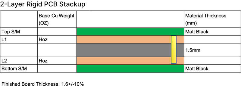
- Suitable for simple, low-speed circuits
- Lowest manufacturing cost
- Easy to design and debug
If your design has low component density and runs at low frequency, a double-sided PCB is often enough.
4-Layer PCB
A 4-layer PCB adds two inner layers — typically one ground plane and one power plane.
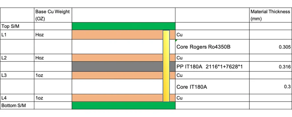
This improves signal integrity and reduces EMI compared to a 2-layer board. It is a popular choice for mid-level designs, like industrial sensors, and basic communication devices. If you need better performance without a significant increase in cost, a 4-layer PCB is a smart step up.
6-Layer PCB
A 6-layer PCB provides more routing space and better signal isolation. It typically includes two signal layers, two ground planes, and two power planes.
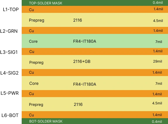
This setup supports cleaner signal routing and more stable power delivery. Industrial control boards, mid-range communication equipment, and products that need better EMI control widely use it.
A 6-layer PCB is a good balance between performance and cost for many industrial applications.
8-Layer PCB
An 8-layer PCB is the go-to choice for high-speed designs. With more dedicated ground and power planes, it delivers strong signal integrity and low EMI.
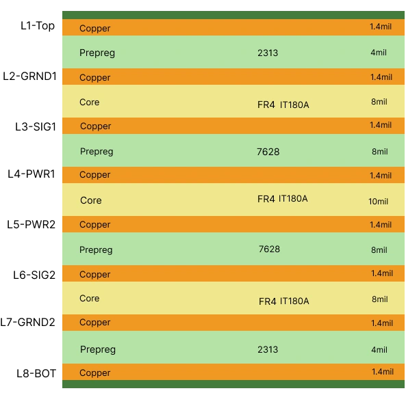
It suits advanced industrial systems, networking equipment, and products running at higher clock speeds. If your design uses high-speed interfaces like DDR, USB 3.0, or PCIe, an 8-layer PCB provides the routing and signal quality you need.
10-Layer PCB
A 10-layer PCB is built for complex, high-performance designs. It supports multiple power rails, strong EMI shielding, and clean signal routing across many layers.
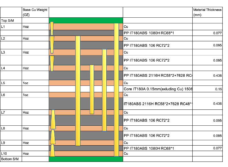
Industrial control systems, telecom equipment, and advanced computing devices commonly use it. When your design demands maximum signal integrity and strict EMI compliance, a 10-layer PCB is the right choice.
12-Layer PCB and Above
For ultra-high-density and ultra-high-speed designs, 12 or more layers may be required. Servers, high-end networking hardware, aerospace systems, and medical equipment use these boards. The added layers allow for more signal routing, better power distribution, and tighter EMI control. If your design falls into this category, a 12-layer PCB or higher may be necessary.
What Adding More Layers Actually Does
Adding layers gives your design three things:
1. More signal layers mean more routing paths.
2. More ground and power planes give your signals smooth and continuous return paths. Better layer separation also reduces noise and interference.
3. Without a solid reference plane nearby, return currents have no clear path to follow. This can cause EMI and signal integrity issues that are hard to fix later.
Key Factors That Determine Layer Count
Signal Integrity
High-speed signals need a solid reference plane nearby to maintain signal quality. Without proper ground and power planes, signals can degrade, causing timing errors and data loss. If your design runs at high frequency, you need more layers to keep signals clean. This is especially important for high-frequency PCB designs where even small impedance variations can cause signal problems.
EMI Requirements
More ground planes mean stronger EMI shielding. If your product must pass FCC, CE, or other EMI tests, add more layers. Use dedicated ground planes, since this is one of the best ways to control emissions. Designs with fewer layers often struggle to meet strict EMI standards without additional shielding.
Power Delivery
If your design uses multiple power rails — such as 3.3V, 5V, and 12V — you need dedicated power planes for each. Sharing power planes between voltage rails causes noise and instability. More layers give you the space to separate power domains cleanly. For designs that need high current, heavy copper PCB technology may be worth considering with your layer count decision.
Component Density
High component density leaves less room for routing traces on each layer. When you pack parts tightly, you need more layers to route all connections.
This avoids crossed signals and design rule breaks. HDI PCB technology uses microvias and fine-pitch routing. It often adds more layers to support intricate designs.
Board Size
Smaller boards have less surface area for routing. When you reduce board size, you often need more layers to fit all the connections. This is common in wearable devices, handheld products, and space-constrained industrial modules.
Board Thickness
Board thickness is the final thickness of a PCB after lamination, plating, and surface finish. Common options include 1.0 mm, 1.6 mm, 2.0 mm, and 2.4 mm. Designers choose thickness based on mechanical strength, component weight, impedance control, and product assembly requirements.
| GENERAL (mm) | MODERATE (mm) | ADVANCED (mm) | |
|---|---|---|---|
| 4L | 0.6-2.5 | 0.5-3.2 | 1.2-8.0 |
| 6-10L | 0.7-2.5 | 0.6-6.0 | 0.5-8.0 |
| 12+ | 1.3-6.0 | 1.2-8.0 |
Budget
Every additional layer adds cost. Material, lamination, drilling, and inspection all become more complex with more layers. Choosing the minimum number of layers that meets your design requirements — not more, not less — is important.
How Engineers Make the Layer Count Decision
Follow these five steps to choose the right layer count for your design:
Step 1: Check Your Signal Speed and Frequency If your design runs below 50MHz, a 2 or 4-layer board may be enough. Above 100MHz, consider 6 layers or more to maintain signal integrity.
Step 2: Count Your Power Rails Each independent power rail benefits from its own plane. If you have three or more power rails, you likely need 6 layers or more.
Step 3: Evaluate Your EMI Requirements. If your product must pass EMI certification, plan for at least two dedicated ground planes. This typically means 6 layers or more.
Step 4: Assess Component Density If your board is small and densely packed, you may need more layers to route all connections cleanly. Create an initial floorplan to evaluate routing requirements.
Step 5: Balance performance with budget.
Once you know the minimum layer count you need, compare it to your budget. If cost is a concern, work with your PCB manufacturer to optimize the stackup before finalizing the design.
The decision is straightforward in practice. If a 2-layer board can handle all your routing cleanly, there is no reason to add more layers. If traces get crowded, signals need long detours, or PCB return paths break up, move to 4 layers or more.
Manufacturing Processes for PCB Layers
PCB layer count is built through a step-by-step manufacturing process. Manufacturers create each layer and then combine the layers under heat and pressure.
First, we pattern the copper foil to form circuit traces. A process called imaging and etching does this. After that, we add an insulating material called prepreg between the layers.
Next, we stack multiple layers together. A process called lamination uses heat and pressure. This bonds all layers into one solid board.

After lamination, technicians drill holes to connect different layers. Then we plate these holes with copper so electricity can flow between layers.
For high-layer PCBs like 8-layer, 10-layer, or 12-layer boards, we repeat this process under stringent control. Small mistakes in alignment or pressure can affect performance.
Modern factories use advanced machines, like laser direct imaging (LDI) and precision lamination presses. They help align each layer correctly.
This is why higher layer PCBs require more advanced manufacturing technology and tighter process control.
Why Work With an Experienced PCB Manufacturer
Choosing the right layer count is easier when you work with an experienced manufacturer. A good manufacturer will review your design and check your stackup. They will recommend the best layer count for your needs and budget.
HXD offers full DFM review for every order. Our engineering team checks your Gerber files, stackup, and impedance requirements before production starts. This helps catch problems early and ensures your board performs as designed.
Whether you need a quick prototype or a large production run, HXD can help. HXD has the experience and equipment to deliver consistent quality.Check our manufacturing capabilities to see what we can do. Or use our PCB trace width calculator to confirm your trace sizes before you order.
If you are unsure about your design, working with an experienced manufacturer can significantly improve reliability and reduce development risk.
Conclusion
No fixed rule exists for PCB layer count. The correct choice depends on:
- Signal speed
- Power complexity
- EMI requirements
- Component density
- Budget constraints
The key principle is simple:
Use the minimum number of layers that fully meets electrical and mechanical requirements.
FAQ