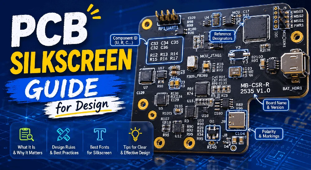
PCB Silkscreen Guide for Design and Manufacturing
Introduction
PCB silkscreen is a marking layer that helps people identify key information on a printed circuit board. It does not carry current. It does not affect the circuit directly. However, a clear silkscreen PCB design helps people read, assemble, test, repair, and identify the board.
This guide explains what PCB silkscreen is, why it matters, and how to design it correctly. You will also learn how to choose the best font for PCB silkscreen.
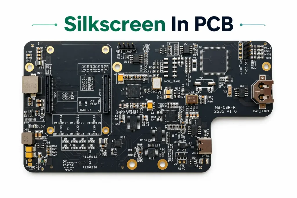
What Is Silkscreen in PCB?
In PCB design and manufacturing, people also call silkscreen the legend layer or component legend.
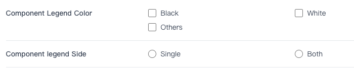
On our quotation page, “Component Legend” means PCB silkscreen. The options “Component Legend Color” and “Component Legend Side” let you choose the silkscreen color and printing side.
Silkscreen includes component marks, symbols, logos, warning labels, and other useful information printed on the board surface.
Common silkscreen content includes:
| Silkscreen Content | Examples |
| Component marks | R1, C1, U1, D1, Q1 |
| Polarity marks | +, -, diode direction, Pin 1 mark |
| Connector labels | VIN, GND, TX, RX, USB |
| Test point labels | TP1, TP2, 3V3, GND |
| Board information | Product name, revision, date code, logo |
Silkscreen can also include general board information.
Examples include:
- Board name
- Part number
- Revision number
- Date code
- Manufacturer logo
- Customer logo
- Warning labels
- QR code
- Serial number
- UL mark
For mass production, board revision and part number are essential. They help prevent mixed versions during assembly and shipment.
PCB silkscreen colors depend on the solder mask color and the options offered by the PCB factory.
The most common silkscreen colors are:
| Silkscreen Color | Common Use |
| White | Most common option for green, blue, red, and black solder mask |
| Black | Often used on white solder mask |
| Yellow | Sometimes used for special designs |
| Other colors | Usually need special confirmation with the PCB manufacturer |
PCB Silkscreen Manufacturing Methods
PCB manufacturers use different methods to print silkscreen. The printing method can affect cost, lead time, and text clarity.
Screen Printing
Screen printing is a traditional silkscreen method. It uses a mesh screen to transfer ink onto the PCB surface.
This method works well for standard PCB production and larger batch orders. It is cost-effective, but it may not be the best choice for very fine text.
LPI
LPI(Liquid Photo Imaging) uses photoimageable ink and exposure process steps. It can produce finer and more accurate markings than traditional screen printing.
LPI is a good choice when the PCB needs clearer text, finer details, and better alignment.
Inkjet Printing
Inkjet printing is a digital printing method. It prints text and symbols directly onto the PCB.
It is suitable for quick-turn production, prototypes, and variable markings such as serial numbers or QR codes.
Different PCB manufacturers may use different silkscreen methods. Designers should always check the manufacturer’s capability before using very small text, fine graphics, or special marks.
PCB Silkscreen Design Guidelines
Good silkscreen design should be clear, useful, and manufacturable.
Keep Text Clear and Readable
Silkscreen text should be large enough to read after manufacturing.
Tiny text may look fine in CAD software, but it may become blurred or broken on the real PCB.
For most standard PCB designs, a safer choice is:
- Font height: 1.0 mm or larger
- Stroke width: 0.15 mm or larger
JLCPCB states that silkscreen text should use at least 1 mm height and no less than 0.15 mm width or spacing between letters. These values are useful references, but you should always confirm the final rule with your PCB manufacturer before production
Avoid Placing Silkscreen on Pads
Do not place silkscreen over solder pads.
Silkscreen on pads may affect soldering. The manufacturer can also remove it automatically during DFM cleanup. If this happens, the final board may lose part of the text or symbol.
For example, if the letter R1 touches a resistor pad, the manufacturer may clip the text. The result may look unclear on the final board.
Keep Enough Clearance from Solder Pads
Silkscreen should keep enough clearance from solder pads, vias, and exposed copper.
A practical rule is to keep silkscreen away from pads by at least the manufacturer’s minimum clearance.
For standard boards, keep about 0.15 mm between silkscreen and solder pads as a general reference. The final rule depends on your PCB factory, so check its DFM rules before production.
Use Consistent Reference Designators
Use standard and consistent designators.
Common examples:
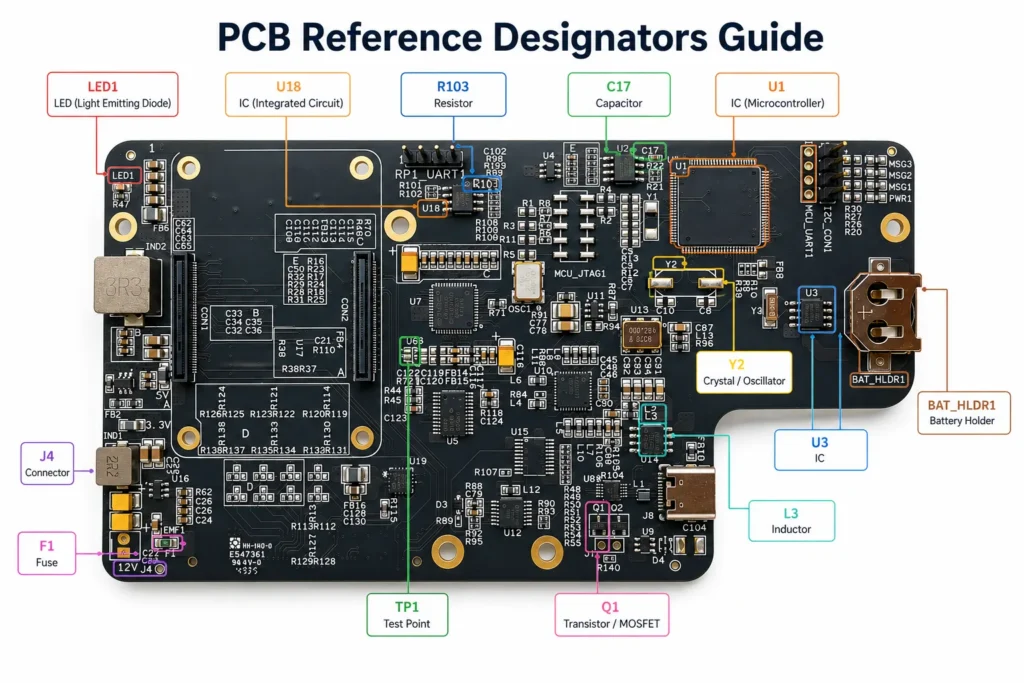
| Component Type | Designator |
| Resistor | R |
| Capacitor | C |
| Integrated circuit | U |
| Diode | D |
| Transistor | Q |
| Connector | J |
| Inductor | L |
| Test point | TP |
| Fuse | F |
Consistent labels make the PCB easier to compare with the schematic, BOM, and assembly drawing.
Adding Custom Logos and Graphics
Custom logos, icons, and graphics can be added to PCB silkscreen.
They are useful for:
- Brand identity
- Product identification
- Warning symbols
- QR codes
- Serial numbers
- Assembly marks
However, logos and QR codes must follow manufacturing limits. Extremely thin lines, tiny spaces, or low-contrast graphics may not print clearly.
For QR codes, confirm the minimum size with the PCB manufacturer. A QR code that is too small may not scan after printing.
Minimum Font Height and Stroke Width
The table below gives practical design references for standard PCB silkscreen.
| Item | Practical Minimum | Safer Recommendation |
| Font height | 0.8–1.0 mm | 1.0–1.2 mm |
| Stroke width | 0.15 mm | 0.18–0.20 mm |
| Pad-to-silkscreen clearance | 0.15 mm | 0.20 mm or more |
| Logo line width | 0.15 mm | 0.20 mm or more |
| QR code size | Depends on data size | Confirm with manufacturer |
These values are general references. The real limit depends on solder mask color, silkscreen color, board surface, printing method, and manufacturer capability.
Font Size Recommendations by Fab
| Source / Fab | Minimum Text Height | Minimum Stroke Width / Line Width | Notes |
| HXD | 1.0 mm | 0.15 mm | Also recommends letter spacing no less than 0.15 mm |
| Standard safe design | 1.0–1.2 mm | 0.18–0.20 mm | Better for readability and fewer DFM issues |
Each PCB manufacturer may have different silkscreen design rules. The safest approach is to check your chosen manufacturer’s latest guidelines before production.
Best Font for PCB Silkscreen
The best font for PCB silkscreen is simple, clean, and easy to read.
A good silkscreen font should remain clear after printing, solder mask processing, assembly, and inspection.
Good choices include:
- Sans-serif fonts
- Vector fonts
- Simple CAD fonts
- Single-line or stroke fonts supported by your EDA tool
Avoid decorative fonts, very thin fonts, and complex logo-style text.
Conclusion
A good silkscreen design should be clear, accurate, readable, and manufacturable. It should also avoid pads, keep enough clearance, and follow the PCB manufacturer’s design rules.
If your PCB needs special silkscreen requirements, such as logos, QR codes, serial numbers, UL marks, or custom graphics, confirm them with your PCB manufacturer before production.
FAQ
Frequently Asked Questions
Is PCB silkscreen necessary?
What is the difference between PCB silkscreen and solder mask?
What is the best font for PCB silkscreen?
Avoid decorative or very thin fonts.
What is the minimum PCB silkscreen font size?
For better readability, 1.0–1.2 mm text height and 0.18–0.20 mm stroke width are safer choices. Always check your PCB manufacturer’s rules.