Prepreg and Core in PCB: Differences, Stackup Design, Material Selection, and Manufacturing Impact
Introduction
When engineers talk about PCB stackup, two terms appear again and again: core and prepreg. They are both dielectric materials, but they are not interchangeable. They have different roles on the board. They act differently during lamination. This affects impedance, manufacturing, and reliability in various ways.
If you make multilayer boards, controlled-impedance designs, HDI boards, you need to learn more. You also need to know how core and prepreg affect final pressed thickness, signal integrity, resin flow, yield, cost, and lead time.
This guide explains all of that in practical terms.
What Are Prepreg and Core in PCB Manufacturing?
In PCB manufacturing, core provides the rigid base. Prepreg bonds the layers together and provides dielectric separation.
Without core, the structure loses stability. Without prepreg, the layers cannot bond together properly.
Quick comparison: core vs prepreg
| Property | Core | Prepreg |
|---|---|---|
| Cure state | Fully cured | Partially cured before lamination |
| Copper | Usually copper-clad on both sides | Normally no copper attached |
| Main role | Structural dielectric base | Bonding and insulating layer |
| Thickness stability | Relatively stable | Changes during lamination |
| Resin flow | No | Yes |
| Impedance predictability | Higher | More process-dependent |
| Typical use | Inner-layer base | Between layers during press |
Core vs Prepreg: The Differences That Matter Most
Curing state: B-stage vs C-stage
Core is already fully cured, which is often called C-stage. Its thickness and shape are relatively stable.
Prepreg starts in B-stage. During lamination, its resin softens, flows, fills the spaces between copper features, and then cures. This means the prepreg thickness listed on paper may not be the same as the final dielectric thickness in the finished PCB.
Electrical Differences Between Core and Prepreg
Core is already cured and stable. It gives more predictable dielectric spacing for impedance control.
Prepreg can also be used in impedance-sensitive structures. But its final thickness can change during lamination. It depends on resin content, glass style, copper density, lamination pressure, temperature, and resin flow.
For this reason, designers should confirm prepreg-based spacing with the PCB fabricator before routing.
Thickness behavior before and after lamination
Core thickness is typically near the specified finished value. This is true except for normal manufacturing tolerances.
Standard core thickness include 0.10, 0.20, 0,4, 0.6, 0.8 and 1.00mm.
Prepreg thickness is different. A prepreg sheet lists a nominal thickness in the datasheet. However, after lamination, the final pressed thickness can change quite a bit. That difference becomes even more obvious in boards with uneven copper distribution or heavy copper features.
| COMMON PREPREG THICKNESS (TOLERANCE AS PER IPC-4101 B/L) (mm) | |
|---|---|
| 7628 (50%) | 0.22 |
| 7628 (43%) | 0.18 |
| 2116 (52%) | 0.12 |
| 2116 (56%) | 0.13 |
| 1080 (65%) | 0.08 |
| 106 (75%) | 0.05 |
Where Core and Prepreg Sit in a PCB Stackup
To understand stackup design, it helps to look at how these materials are used in actual board constructions.
This is a real 4-layer stackup from HXD production.
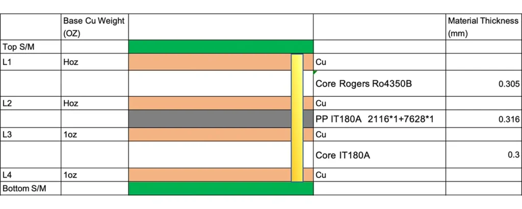
In this structure, the central core acts as the rigid dielectric foundation, while prepreg bonds the outer copper foil to the core.
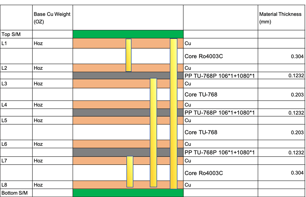
As layer count increases, such as 8-layer designs, the stackup becomes more sensitive to symmetry, resin flow, and registration. In high-speed designs, the exact placement of core and prepreg matters more because it affects impedance, lamination stability and via structures.
Buried vias and sequential lamination
In HDI designs, stackup design becomes more complex because the board may be laminated in more than one cycle. Sequential lamination affects how we choose prepreg and core materials. They need to withstand repeated heat cycles and stay aligned through several build stages.
Why core layers often provide more stable impedance
One of the biggest reasons designers care about prepreg and core is impedance.
Core layers usually provide more stable dielectric spacing. The material is already cured, so its thickness is more predictable.
When a trace is routed over a reference plane through a core dielectric, the impedance is often easier to control. This makes core-based stripline structures useful for tight impedance targets.
This does not mean prepreg is bad for impedance control. It only means core is often easier to model and keep consistent during production.
Nominal Prepreg Thickness Is Not Final Thickness
This point deserves its own section because The same prepreg can press differently in different PCB designs. A standard communication board and a heavy-copper power board may not get the same final dielectric thickness. This can happen even when they use the same prepreg part number.
The final pressed thickness depends on:
- lamination pressure
- lamination temperature profile
- resin content
- copper thickness
- copper pattern density
- number of prepreg plies
- adjacent material roughness
Some boards need controlled impedance. HDI boards are a good example. Designers should confirm the pressed dielectric thickness with the PCB fabricator before finalizing the stackup.
Storage, Handling, and Moisture Control
Another under-discussed topic is material handling before lamination.
- Prepreg shelf life matters – Prepreg is a process-sensitive material. It does not behave the same forever in storage. Age, storage temperature, and humidity can change how it flows and cures.
- Moisture absorption – If prepreg absorbs too much moisture, it can affect lamination quality and increase the risk of voids or bonding issues.
- Shop-floor handling – Before use, prepreg needs proper storage and careful handling. In some cases, it should return to room temperature before pressing. These details affect consistency.
- Process window – Every prepreg system has a useful process window. If material is stored too long or handled poorly, the lamination result may become less predictable.
Designers and buyers should remember this key point: the quality of the finished PCB relies on both the stackup design and how well the material is managed during production.
How to Choose Between Core and Prepreg in Real Projects
The best approach is not to ask whether core is better or prepreg is better. The better question is: what combination supports the board’s electrical, mechanical, and manufacturing needs?
A practical decision framework
Ask these questions:
- Is the board standard multilayer, high-speed, RF, HDI, or heavy copper?
- Are there strict impedance targets?
- Will the board require sequential lamination?
- Does the design need tight thickness control?
- Is low loss more important than low cost?
- Can the chosen material family be sourced easily by the intended fabricator?
- What material families do you normally stock?
- What pressed dielectric thickness do you expect for this stackup?
- Can you support this impedance target with your standard materials?
- Do you recommend a different prepreg style or ply count?
- Will this structure affect lead time or yield?
Conclusion
Core and prepreg are both essential to multilayer PCB construction, but they serve different purposes. Core provides the stable, rigid dielectric building block. Prepreg provides the bonding and insulating layer that forms the final laminated structure.
For simple boards, the difference may seem academic. For controlled-impedance, HDI, high-speed, RF, or high-reliability designs, this is an important factor. It affects both design and manufacturing.
The most important practical lessons are these:
- core and prepreg are not interchangeable
- prepreg nominal thickness is not finished dielectric thickness
- impedance accuracy depends on real pressed values, not generic charts
- material choice affects yield, lead time, cost, and reliability
- the best stackup is the one that balances performance with manufacturability
If you are designing a multilayer or impedance-controlled PCB, do not finalize the stackup based only on datasheets or generic online tables. Confirm the actual pressed dielectric structure with your PCB fabricator before release. That one step can prevent costly redesigns, impedance problems, and production delays.
FAQ