PCB Stackup Design Guide for Multilayer Boards
Introduction
PCB stackup design is not just about arranging copper layers. It affects signal integrity, power stability, EMI control, heat management, board thickness, cost, and manufacturing reliability.
This guide explains the main parts of PCB stackup design. It covers multilayer structures, and practical design rules.
Key Elements in a PCB Stackup
Copper Layers

Copper layers are used for signal routing, power distribution, and grounding.
Signal layers carry high-speed signals, low-speed signals, and general circuit connections. These layers should have a clear reference plane nearby when impedance or EMI control is important.
Ground planes provide stable return paths for signals. They also help reduce noise and improve EMI performance.
Power planes distribute power across the PCB. When placed close to ground planes, they can help reduce power noise and improve power stability.
Core and Prepreg
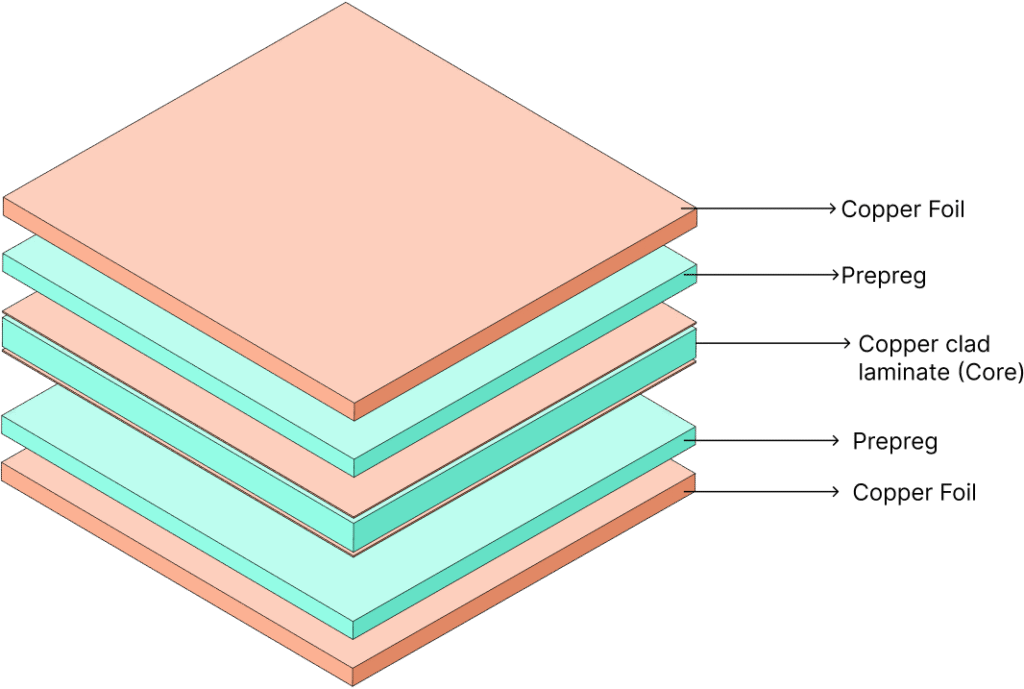
Core and prepreg are the main insulating materials in a PCB stackup.
A core is a cured dielectric material. It usually has copper on one or both sides.
A prepreg is a semi-cured fiberglass resin sheet. Lamination places it between layers and bonds the layers together. Under heat and pressure, the resin flows and fills the space between copper layers.
In simple terms, core provides structure, while prepreg bonds the layers together.
If you already understand PCB stackup design, you can use our PCB Stackup Design Tool to work faster and easier.

It lets you see layers, vias, and impedance in a clear visual way. You can also export your design as CSV, JSON, or PDF files. This helps you check your stackup, share it with others, and use it in design reviews or manufacturing.
Common Multilayer PCB Stackup Structures
PCB stackup structure depends on layer count, signal speed, power needs, board thickness, and manufacturing limits. Below are several common multilayer PCB stackup structures we often use.
6-Layer PCB Stackup
A 6-layer PCB is a practical choice for designs that need more routing space than a 4-layer board. Compared with a 4-layer PCB, a 6-layer stackup can provide more stable power distribution and better EMI control.

Designers can use dedicated ground and power planes to create shorter return paths and reduce noise.
8-Layer PCB Stackup
An 8-layer PCB works well for designs needing dense routing, high-speed signals, multiple power zones, and improved EMI control. It gives PCB designers more freedom to separate signal layers, ground planes, and power planes.
PCB manufacturers often choose 1.6 mm, 2.0 mm, or 2.4 mm as the finished thickness for 8-layer PCBs.

10-Layer PCB Stackup
A 10-layer PCB is used for more complex electronic systems. It is suitable for servers, communication equipment, FPGA boards, BGA designs, high-speed interfaces, and advanced industrial products.
The main advantage of a 10-layer stackup is greater routing freedom. Designers can use more signal layers, stronger ground reference structures, and better power plane planning.

We do not provide fixed PP types because prepreg selection depends on your design, copper distribution, and stackup requirements. Each factory may choose different prepreg types or combinations based on its own production process.
PCB Stackup Design Rules
A good PCB stackup should balance electrical performance, mechanical stability, and manufacturing reliability. This helps reduce design changes and production risks. Based on years of experience, We have summarized the following key points for you.
1. Keep the Stackup Symmetric
A PCB stackup should be as symmetric as possible from the center line. This includes copper weight, dielectric thickness, and material arrangement.
A symmetric stackup helps reduce internal stress during lamination and reflow soldering. It also lowers the risk of PCB warpage. This is especially important for multilayer PCBs, thin boards, and designs with BGA or fine-pitch components.
2. Choose Foil Build for Standard Stackups
Most standard multilayer PCB stackups use a foil build structure. This is a common and stable manufacturing method.
A special core build is also possible, especially when using high-frequency materials such as Rogers. However, it is less common and usually needs extra engineering review. For standard FR-4 multilayer PCBs, foil build is often the more practical choice.
3. Control Dielectric Thickness
Before routing, designers should confirm the dielectric thickness for controlled impedance, high-voltage, or HDI designs.
If the fabrication drawing does not specify dielectric thickness, designers can use 90 μm as the minimum reference according to IPC, as long as the design does not include microvias.
4. Consider Thickness Tolerance
For boards thicker than 1 mm, the standard thickness tolerance is ±10%. For 1.0 mm boards, the standard thickness tolerance is ±0.1 mm.
For boards 1.0 mm or thinner, the thickness tolerance should be confirmed and approved by PCB manufacturer before production.
5. Do Not Use Too Many Prepreg Sheets
Prepreg is used to bond copper layers and cores together during lamination.
A practical rule is to use no more than 3 prepreg sheets for bonding layers together. Too many sheets may make resin flow harder to control and can increase thickness variation after pressing.
6. Allow for Production Stackup Adjustment
The stackup used in production may be slightly different from the original design proposal. This can happen because of copper distribution, available materials, prepreg resin content, or factory process strategy.
A reliable PCB manufacturer should send an EQ before starting production if they need changes. Designers should review and approve the final production stackup before fabrication starts.
7. Check Prepreg Resin Content
Even the same prepreg type can have different resin percentages. This can affect the final pressed thickness of the prepreg.
For controlled impedance or tight thickness designs, do not ignore resin content. The final dielectric thickness after pressing may differ from the nominal prepreg thickness.
8. Review Microvia Aspect Ratio
If the PCB design uses microvias, the prepreg thickness must support reliable laser drilling and plating.
A common recommended microvia aspect ratio is about 0.8:1. More advanced processes may support 1:1, but confirm this with the manufacturer before finalizing the stackup.
9. Vias Types
PCB vias play a key role in PCB stackup design because they connect signals between different copper layers.
They allow current and signals to move up and down through the board, which makes compact and high-performance designs possible. If you want to learn more, you can read this guide on PCB vias.
In our PCB Stackup Design Tool, you can visually create different types of vias.
10. Impedance control
It is important to note that PCB stackup has a direct impact on impedance control. The distance between the signal layer and reference plane, copper thickness, and material Dk all affect the final impedance value. For more details, read our guide to Impedance Control.
If your project requires special materials, tight thickness tolerances, or custom stackups, please contact us for engineering support.
PCB Stackup parameters
Foil thickness after processing is not always the same as the base foil thickness. During PCB manufacturing, inner-layer copper may become thinner after etching. Outer-layer copper usually becomes thicker after plating.
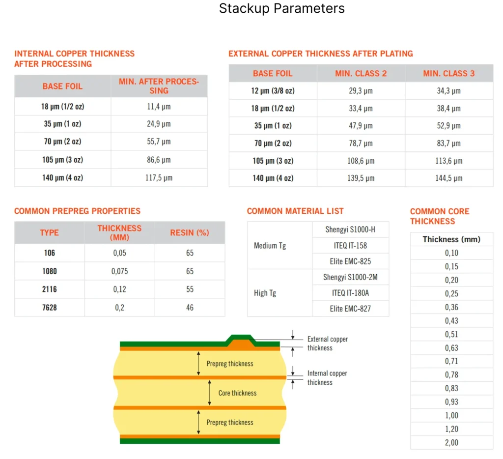
When designing a multilayer PCB, confirm these stackup parameters with your PCB manufacturer before routing. This helps avoid impedance errors, and production issues.
Conclusion
Choose the PCB stackup based on layer count, signal speed, impedance needs, power requirements, board thickness, material type, cost, and manufacturing capability. For high-speed, HDI, RF, or rigid-flex designs, review the stackup with your PCB manufacturer early.
If your project needs multilayer PCB stackup support, We can help review your design, recommend suitable materials, calculate impedance, and confirm a manufacturable stackup before production.
FAQ