Telecom PCB Manufacturing: Complete Guide to Materials, Design
Introduction
For PCB designers, telecom PCB projects can be challenging. These boards require strict control over signal quality, impedance tolerance, and heat dissipation. Even small changes in material or trace width can affect performance. For this reason, telecom PCB manufacturing needs careful planning, stable processes, and strict quality control.
This guide explains the key points in telecom PCB manufacturing. It covers materials, design rules, and manufacturing challenges.
Why Telecommunication PCBs Are Different
Most telecom products work at high speed, high frequency, or high power. This makes both PCB design and telecom PCB manufacturing much more difficult.
1. High-Speed Signal Transmission
Telecom PCBs often handle high-speed digital signals. High-speed signals are affected by many factors, such as trace impedance, return path, and crosstalk.
Even a small layout issue can affect signal quality and lead to data errors. That is why telecom PCB design requires controlled impedance and a stable layer stackup.
2. High-Frequency and RF Performance
Wireless communication, 5G equipment, antenna modules, and RF front-end circuits often use high-frequency signals.
In a high frequency PCB for telecom, signal loss must be carefully controlled. The choice of material plays a key role. Dk, Df, and lamination structure can all affect signal quality.
For RF and microwave applications, standard FR-4 may not provide enough performance. You may need Rogers laminates, PTFE materials, or hybrid stackups for better high-frequency performance.
3. EMI and EMC Control
Telecommunication equipment often works in a complex electrical environment. High-speed digital circuits, RF circuits, and power circuits may create noise.
A good telecom PCB uses proper stackup design, ground planes, shielding, and power integrity control to reduce EMI risk.
4. Thermal Management
Base stations, servers, and power amplifier modules can generate a lot of heat. Common thermal management techniques used in telecom circuit boards include:
• Thicker copper layers in high-current areas
• Thermal vias for vertical heat transfer
• Large copper pour zones
• Metal core materials for high-power modules
• Optimized stackup planning to distribute heat evenly
If your telecom product runs for long hours, you should review thermal design before final routing.
Materials for Telecom PCB
Material choice affects signal speed, signal loss, heat resistance, and cost. Choosing the right material is one of the most critical decisions in telecom PCB manufacturing services.
FR-4
FR-4 is the standard choice for many telecom rigid pcb designs that do not require RF-grade performance. It has good mechanical strength, good insulation, and lower cost.
FR-4 works well for:
- Basic communication modules
- Low-speed control boards
- Cost-sensitive telecom products
- Standard multilayer PCBs
But FR-4 may not be the best choice for high-frequency or high-speed circuits. At higher frequencies, FR-4 can cause more signal loss.
High-Tg FR-4
High-Tg FR-4 handles heat better than standard FR-4. It works well for multilayer telecom PCBs and industrial communication products.
Choose it when your board needs better heat resistance but does not need RF-grade material
Rogers / PTFE Materials
Rogers and PTFE materials are common in 5G, antenna, RF, and satellite communication applications. They provide stable high-frequency performance, lower signal loss, and stable Dk/Df values.
For high frequency PCB for telecom applications, these materials can also support tight impedance control, such as ±3% or better for demanding RF designs. However, they cost more than standard FR-4 and need tighter process control during drilling, lamination, and surface treatment.
Metal Core Materials
Metal core materials help move heat away from high-power circuits. They are useful in power amplifier modules, LED communication devices, and other high-heat telecom modules.
Not every telecom product needs a metal core PCB. You should choose it when high-power circuits need better heat control.
Design Guidelines for Telecom PCB
1. Use Continuous Ground Planes
High-speed signals need a stable return path. You should avoid cutting the reference plane under high-speed traces.
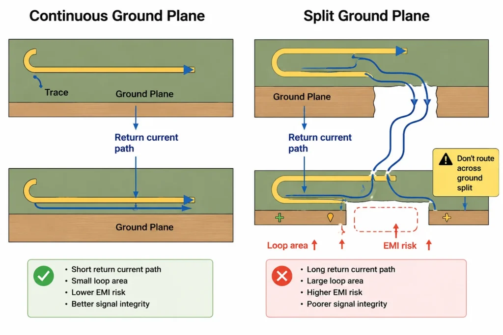
A continuous ground plane can reduce EMI and improve signal quality. It also gives the PCB a cleaner current return path.
2. Keep High-Speed Traces Short and Controlled
When you design high-speed traces, you should keep critical signal paths short and direct. Long traces can increase signal loss, reflection, and crosstalk.
You also need to follow the controlled impedance rules from the stackup, such as line width, spacing, copper thickness, and dielectric thickness.
3. Control Differential Pair Routing
Differential pairs are fundamental to many telecom interfaces, including Ethernet, PCIe, USB, SERDES, and high-speed data links. Key routing parameters to control include:
• Pair spacing and symmetry
• Length matching between the positive and negative traces
• Differential impedance (typically 100Ω ±10%)
• Reference plane continuity under the pair
• Via transition geometry and stub length
If you use differential pairs, you should confirm the impedance target and stackup with your PCB manufacturer before final routing.
4. Separate RF, Analog, Digital, and Power Areas
Different circuit blocks should have clear layout zones. RF circuits, analog circuits, digital circuits, and power circuits should not mix without control.
This layout method reduces noise coupling. It also makes testing and troubleshooting easier.
When you plan the layout, place sensitive RF and analog sections away from noisy switching power areas.
5. Manage Heat Early
You should start thermal design before final routing. Identify hot components early, such as power ICs, processors, and power modules.
Use thermal vias, copper areas, proper component spacing, and heat sink zones when needed.
6. Work with the Manufacturer Before Finalizing Stackup
Controlled impedance is a shared responsibility between the designer and the PCB manufacturer. Before finalizing the stackup, confirm the following parameters directly with your telecom PCB manufacturing partner:
• Laminate material and grade
• Copper thickness per layer
• Dielectric thickness between layers
• Trace width and spacing for each impedance target
• Impedance tolerance (typically ±5% or ±10%)
• Test coupon design and placement
Early alignment on these parameters reduces redesign risk and prevents production delays caused by stackup mismatches.
7. Use Hybrid Stackup When Needed
Some high-frequency telecom PCBs use hybrid stackups. This means the PCB combines different materials in one board.
Common hybrid configurations include:
- Rogers + FR-4
- PTFE + FR-4
- High-speed FR-4 + standard FR-4
A hybrid stackup can balance performance and cost. Critical RF or high-speed layers use low-loss material. Other layers use standard materials to control cost.
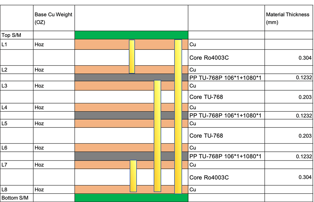
HXD has rich experience in hybrid PCB manufacturing. Learn more from our 8-layer PCB stackup examples for high-speed and impedance-controlled designs.
Need help applying these design guidelines? Send your requirements to us.
Telecom PCB Manufacturing Challenges
Telecom PCB manufacturing services require tight process control at every production stage. These boards often use fine-line routing, controlled impedance, high layer counts, and specialty materials. Because of this, the manufacturer must control each production step carefully.
1. Fine Lines and Dense Routing
Telecom PCBs often have high component density. Small components, dense connectors, and high-speed ICs may require fine lines and small spacing.
Manufacturers need stable imaging, etching, and AOI inspection. If the process drifts, traces may become too narrow, too wide, or shorted.
2. Controlled Impedance in Telecom PCB Manufacturing
Impedance control depends on both design and production. The final impedance can change because of pressed dielectric thickness, copper thickness, etching results, and plating variation.
A reliable telecom PCB manufacturer should review the stackup before production. They should also use TDR testing when the board requires impedance verification.
3. Via Reliability
Multilayer telecom PCBs often use several via types, including:
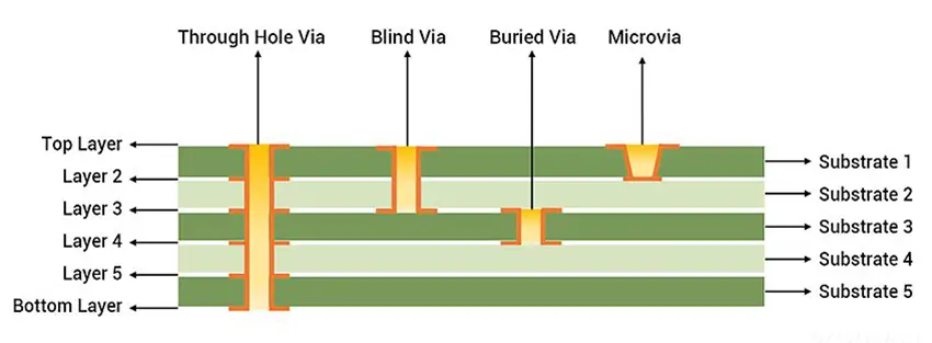
- Through-hole vias
- Blind vias
- Buried vias
- Microvias
- Via-in-pad
Via plating quality directly affects reliability. Poor plating can cause open circuits, cracks, or failure after thermal cycling.
For HDI telecom PCB projects, microvia quality and layer-to-layer alignment are especially important.
4. Lamination Control
Multilayer telecom PCBs need stable lamination. The manufacturer must control dielectric thickness, resin flow, layer alignment, and void risk.
Poor lamination can cause delamination, impedance shift, or reliability problems. This risk increases when the board uses high layer counts, mixed materials, or thin dielectric layers.
5. Material Processing
Rogers, PTFE, and hybrid materials are harder to process than standard FR-4. They need better drilling, desmear, lamination, and dimensional control.
A supplier with only standard FR-4 experience may struggle with high frequency PCB for telecom projects. Material handling skill matters.
6. Thermal Stress
Telecommunication equipment may run for long hours. The PCB must handle heat from operation, lead-free soldering, and thermal cycling.
Material selection, copper balance, via design, and lamination quality all affect thermal reliability.
Conclusion
For telecom PCB manufacturing services, the manufacturer must control more than board fabrication. They must manage impedance, lamination, via reliability, material processing, and testing.
A reliable telecom PCB starts with the right design decisions. It also depends on a manufacturer that understands materials, stackup, signal integrity, and quality control.
If you have a telecom PCB project, contact HXD to discuss your requirements and receive a detailed quotation.
Send your Gerber files to HXD for telecom PCB quotation.
FAQ
Frequently Asked Questions
What Is a Telecom PCB?
How HXD Controls Quality for Telecom PCB Manufacturing?
AOI
Electrical testing
Flying probe testing
TDR
Micro-section analysis
X-ray inspection
Ionic contamination testing
Peel strength testing
First Article Inspection
What Telecom PCB Manufacturing Capabilities Does HXD Offer?
• Layer count: 2 to 20+ layers
• Controlled impedance tolerance: ±5% standard, ±3% available
• Materials: FR-4, High-Tg FR-4, Rogers, PTFE, Polyimide, hybrid stackups
• Via types: through-hole, blind, buried, microvias, via-in-pad
• Surface finishes: ENIG, HASL, Immersion Silver, OSP
• IPC Class 2 and Class 3 manufacturing
• Quick-turn prototype and volume production
What files should I provide for a telecom PCB quotation?
Gerber files
Drill files
Stackup requirements
Material type
Copper thickness
Board thickness
Surface finish,
Impedance targets
Do telecom PCBs always need controlled impedance?
What impedance values are common in telecom PCB design?
The final value depends on the interface, material, stackup, and design requirements.