PCB Specifications Explained: A Buyer’s Guide
When requesting a quotation for printed circuit boards, many buyers focus first on price and lead time. But in practice, a reliable quotation starts with clear and complete PCB specifications. Missing or unclear key PCB order parameters can cause the supplier to make assumptions. This may result in inaccurate pricing, engineering delays, or risks in manufacturability.
In this guide, we help purchasing teams understand key items in PCB quotes and production reviews.
These include layer count, copper weight, board thickness, drill sizes, trace and spacing, solder mask, and surface finish.
Why PCB Specifications Matter When Ordering PCBs
A PCB is not just a file for manufacturing. It is a product built according to a full set of technical requirements. These PCB specifications affect:
- manufacturing difficulty
- raw material selection
- production yield
- electrical performance
- assembly compatibility
- final cost
Making a PCB is not a simple process. It involves many steps—from designing the circuit to drilling holes, adding copper layers, and applying the final coating. At each stage, operators need to set the machines to exact measurements. Even a small mistake can cause the board to fail.
That is why buyers should understand the main PCB order parameters before sending an RFQ. Asking the right questions and knowing what to check can help you avoid costly mistakes. It also reduces rework and ensures the boards you order meet your design needs.
- PCB layer count
- PCB board thickness
- PCB copper weight
- minimum trace/space
- minimum drill size
- surface finish
- solder mask color
- silkscreen or legend
- special requirements such as impedance control, blind vias, buried vias, HDI, or heavy copper
Complete information helps get quotes quickly. It also makes manufacturing reviews more reliable. This is true for both standard and advanced PCB projects.
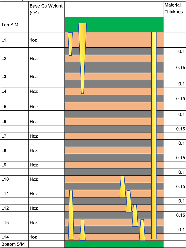
PCB Layer Count
One of the first things a PCB manufacturer checks is the PCB layer count. This tells how many copper layers the board contains and directly affects production complexity.
Common PCB layer count options
1-layer PCB
Also called a single-sided PCB, it has copper on only one side. People usually use it for very simple and cost-sensitive products.
2-layer PCB
Also called a double-sided PCB, it has copper on both sides. A common choice for many standard electronic products.
Multilayer PCB
Any PCB with 4 or more layers is called a multilayer PCB, such as 4-layer, 8-layer, 10-layer, or 12-layer designs. As the number of layers increases, the board can support more complex circuitry and higher routing density. This makes them ideal for industrial equipment, automotive systems, communications, and high-density electronics.
How PCB layer count affects cost
As PCB layer count increases, the board usually requires:
- more prepreg and core material
- additional lamination steps
- tighter registration control
- more inspection during production
This means higher layer count often increases cost and lead time. Buyers should choose a layer count that matches real design needs rather than using unnecessary layers.
At HXD Circuit, we support projects from standard double-sided boards to multilayer, HDI, and rigid-flex PCBs, We help customers balance performance and cost
PCB Board Thickness: Standard 1.6mm and Other Options
Board thickness represents another key part of PCB specifications, and applications often use different options.
Common PCB board thickness options
The most common options are 0.8mm, 1.0mm, 1.2mm, 1.6mm, and 2.0mm. Of these, 1.6mm is the industry standard and works well for most designs. Compact builds use thinner boards like 0.8mm, while projects that need extra rigidity choose thicker options like 2.0mm.
At HXD Circuit, we support board thicknesses from 0.4mm to 3.2mm. This lets you create anything from slim wearables to heavy-duty industrial boards.
Why PCB board thickness matters
PCB board thickness influences:
- mechanical rigidity
- connector matching
- impedance design
- assembly stability
- thermal and structural performance
Thin boards work well in compact devices. Thicker boards are better for products needing more strength. In some designs, engineers must also evaluate PCB board thickness together with copper thickness, drill size, and aspect ratio.
PCB Copper Weight: 1oz vs 2oz vs Heavy Copper
Among all PCB order parameters, PCB copper weight is one of the most important for electrical and thermal performance.
In PCB manufacturing, manufacturers commonly describe copper thickness in ounces per square foot, such as 1oz or 2oz.
Common PCB copper weight options
- 1oz copper: standard for many applications
- 2oz copper: used for higher current or stronger thermal performance
- 3oz and above: often considered heavy copper
How PCB copper weight affects performance and cost
Higher PCB copper weight can improve:
- current carrying capacity
- heat handling
- conductor robustness
But it can also increase:
- etching difficulty
- line width limitations
- process complexity
- production cost
For example, a 2oz PCB may require more careful DFM evaluation than a 1oz board. Heavy copper designs require even more process attention.
At HXD Circuit, we support standard and higher PCB copper weights.These options meet industrial, power, and other demanding PCB needs
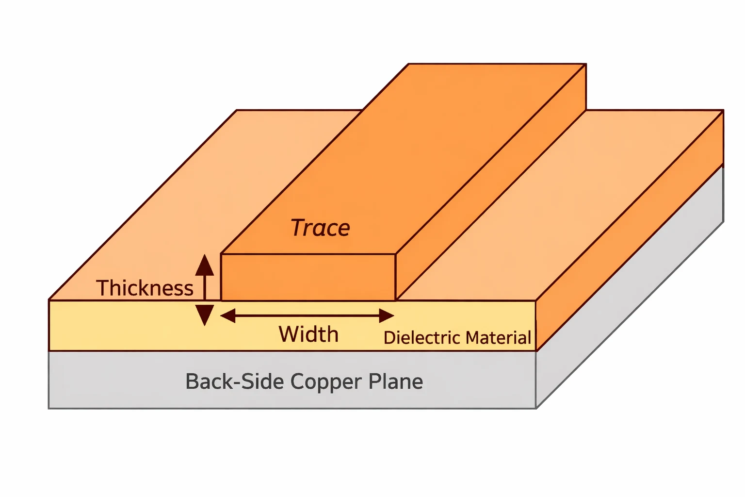
Minimum Trace and Space: A Key Manufacturability Parameter
Minimum trace width and spacing are fundamental PCB specifications because they determine how fine the circuit pattern must be.
Why trace/space matters
Smaller trace and spacing values usually mean:
- higher routing density
- tighter process control
- more advanced manufacturing capability
- potentially higher cost
For standard multilayer PCBs, using common trace and space values is simpler to make. This approach usually lowers costs. For HDI designs or boards with tight routing needs, you may need finer traces and spaces to meet layout demands. However, using overly tight values without a real design need can push your quote higher than it needs to be.
That’s why a manufacturability review matters before you enter production. At HXD, we suggest using our free PCB Trace Width Calculator early in your design. This helps you spot potential issues before they lead to costly changes.
Not Sure Which Specs Are Right for Your Design?
Drill Sizes and Aspect Ratio Limits
Drill information is another important part of PCB order parameters. Buyers usually state the hole size they want. However, the manufacturer must check if drilling and plating are possible.
Why drill size matters
Smaller drill sizes can require:
- tighter drilling accuracy
- more difficult plating control
- stronger process capability
What aspect ratio means in PCB manufacturing
Aspect ratio generally refers to the relationship between PCB board thickness and drilled hole diameter. When the board becomes thick and the hole becomes small, plating reliability becomes more difficult.
This is especially important in multilayer boards and high-reliability applications. That is why you should not review drill size alone. Check it together with the PCB board thickness and the PCB layer count.
Solder Mask Color and Silkscreen Requirements
Solder mask and legend might seem like small details, but they are important. They are part of the full PCB specifications, so include them clearly on the quote form.
- Green
- Black
- White
- Red
- Yellow
- Blue
Green is the most common and usually the most economical option. You may choose other colors to enhance the product’s appearance or support branding.
Silkscreen and legend details
Silkscreen may include:
- reference designators
- polarity marking
- company logo
- part names
- product labels
Customers should also confirm silkscreen color and any special marking requirements in advance.
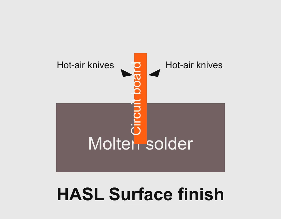
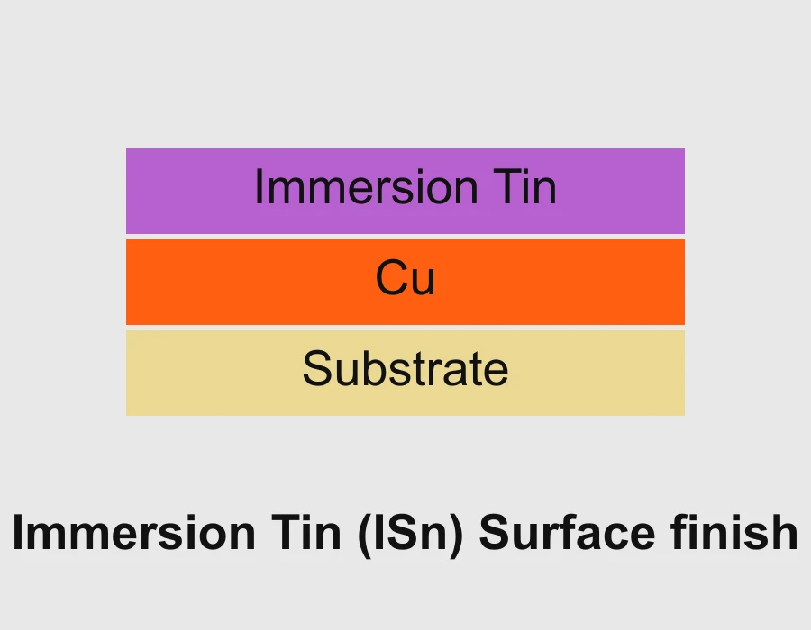
Surface Finish Selection Recap
Surface finish is one of the most important PCB order parameters because it affects solderability, Surface finish is a key PCB order parameter because it affects solderability, flatness, storage life, and cost.
Common PCB surface finish options
The following are commonly used PCB surface finishes.
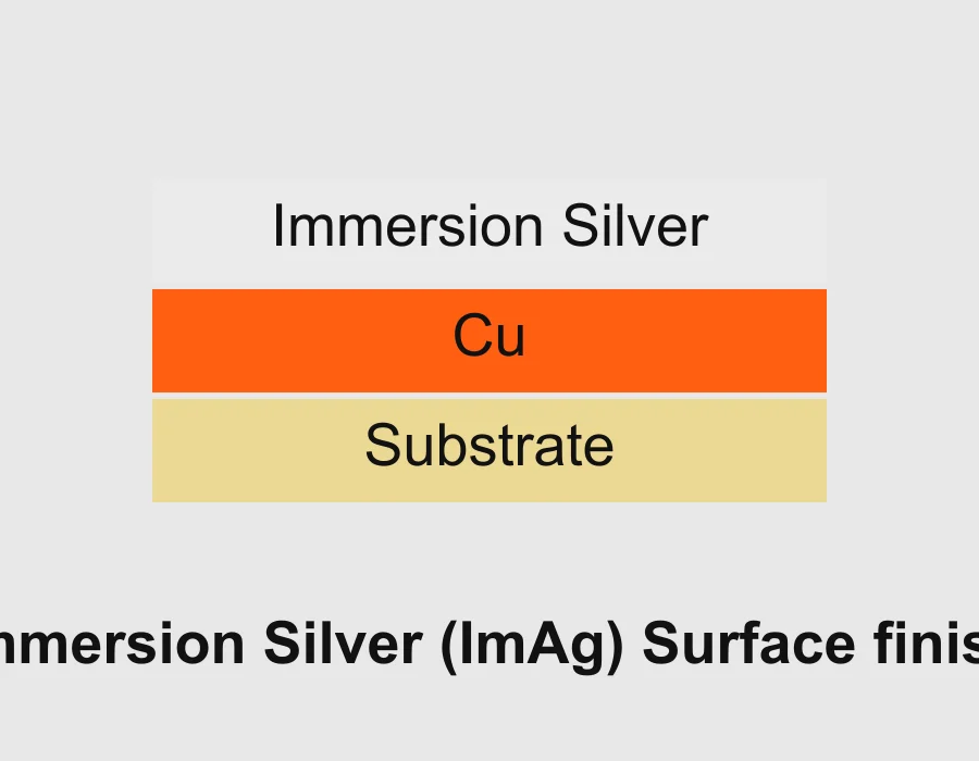
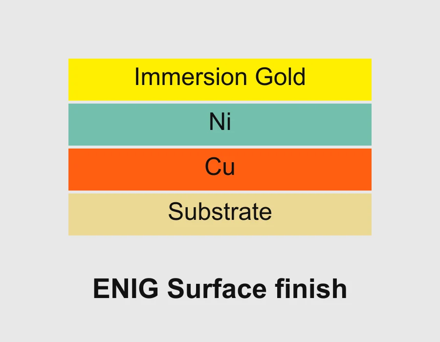
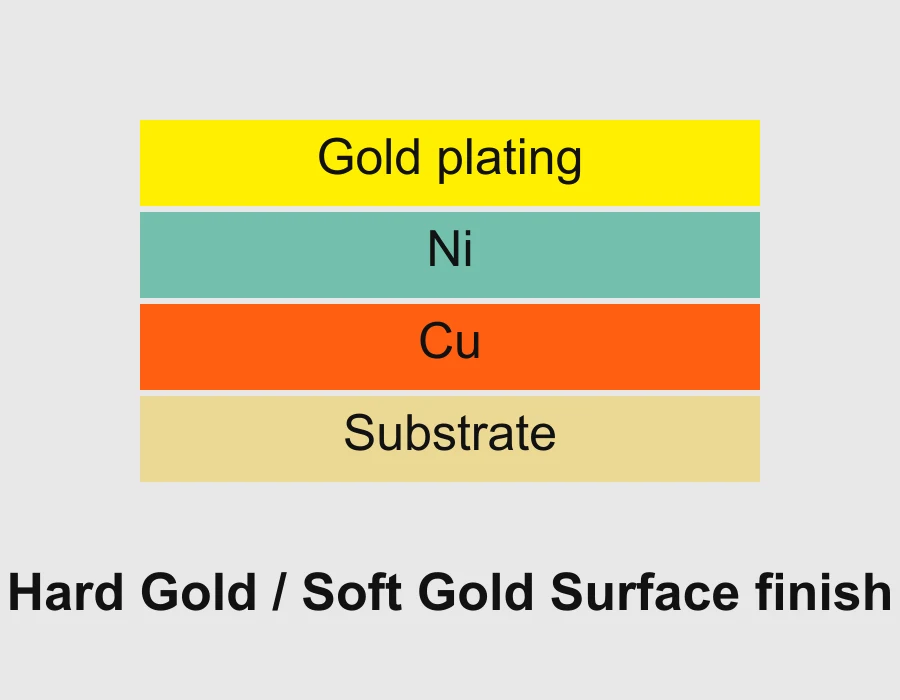
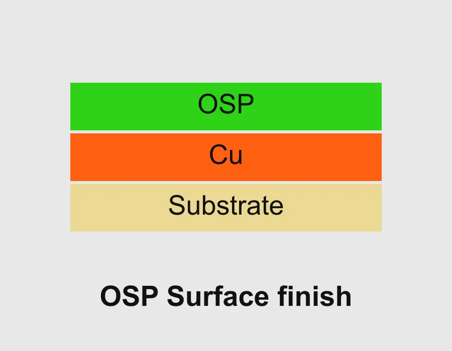
How to choose the right surface finish
Different finishes suit different applications:
- HASL is widely used and cost-effective
- OSP is economical for many standard products
- ENIG provides a flatter surface and is often preferred for finer-pitch assembly
The right surface finish depends on how you assemble, shelf-life needs, budget, and technical specs. You can check all surface finish options here to compare and find the best one for your project.
HXD’s engineering team can help you evaluate your options and find the finish that best balances performance and cost.
Conclusion
The more detailed your PCB specifications are. It is easier for the supplier to provide an accurate quote. It is also easier for the supplier to complete an engineering review.
To simplify the process, HXD’s quote form covers all the key parameters you’ll need. It includes layer count, board thickness, copper weight, material type, surface finish, and more. Just fill in what applies to your design, and our team will take it from there.
Ready to Place Your PCB Order?
FAQ