How to Choose the Right 4-Layer PCB Stackup
Think Deeper with AI:
The best 4 layer PCB stackup does not come from a fixed template. It depends on your circuit, signal speed, board thickness, and manufacturing process. A stackup that works well for a low-speed MCU board may cause trouble in a compact board with a small BGA.
This guide explains how to choose the right 4-layer PCB stackup from an engineering point of view. We will compare common layer structures and discuss signal integrity, EMI control, and impedance control.
Common 4-Layer PCB Stackup Options Compared
Most 4-layer boards use one of several common structures. Each option has a different balance of signal integrity, EMI control, and cost.
| Stackup | Best For | Signal Integrity | EMI Control | Power Distribution | Cost |
| Signal / Ground / Power / Signal | General digital boards | Medium | Medium | High | Low |
| Signal / Ground / Ground / Signal | High-speed and EMI-sensitive boards | High | High | Medium | Medium |
| Signal + Power Pour / Ground / Ground / Signal + Power Pour | Compact high-speed boards | High | High | Medium | Medium |
| Signal / Ground / Mixed Plane / Signal | Mixed-signal designs | Medium to High | Medium to High | High | Medium |
| 4-layer HDI with blind vias | Small BGA or dense modules | High | High | Medium | High |
This table gives a quick view, but the real choice depends on the details of the design.
Signal-Ground-Power-Signal
This is the typical 4 layer PCB stackup used in many digital boards. It is easy to manufacture and cost-effective for standard designs.
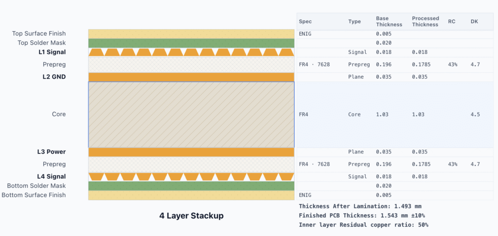
L2 provides a solid ground reference for top-layer signals, and L3 works as a full power plane. This structure makes power distribution easier for boards with multiple ICs and moderate current demand.
This stackup suits general digital boards, MCU control boards, sensor boards, industrial controllers, and many consumer products. If the design has low-speed signals and does not need tight EMI control, this stackup often works well.
The weakness appears on the bottom layer. L4 often uses L3 as its reference plane.
If L3 is a clean and continuous power plane, that may work. But many real boards split L3 into several power islands, such as 5V, 3.3V, 1.8V, and analog power. When a high-speed signal crosses those splits, its return current cannot follow a clean path.
That can create impedance changes, larger current loops, and more radiation.
This stackup can be a good choice, but it requires careful routing. Place high-speed signals on L1 whenever possible, where they can reference the solid ground plane on L2. Avoid routing fast signals on L4 across split power areas. When L4 must carry high-speed signals, make sure each signal has a continuous and clear return path.
Signal-Ground-Ground-Signal
This stackup uses two internal ground planes.
For many high-speed outer-layer designs, this can be the best 4 layer PCB stackup. Both signal layers sit next to a ground plane. That makes return current paths short and predictable.
This structure also supports better EMI control. A nearby ground plane reduces loop area. Smaller loops tend to radiate less. The design also becomes easier to review because both outer signal layers have the same type of reference.
This stackup works well for USB, RF modules, compact digital boards, and products that must pass stricter EMI tests.
The trade-off is power routing. Since both internal layers serve as ground planes, we must distribute power without a dedicated internal power plane.
Power must use local copper pours, wider traces, and via stitching between top and bottom power areas. That approach works well when the board has only a few power rails and moderate current.
For a small board with one main 3.3V rail, this structure may be cleaner than the classic Signal / Ground / Power / Signal stackup. For a complex power board with many rails and higher current, it may create layout pressure.
A dual-ground 4-layer stackup also requires careful decoupling design. Place decoupling capacitors close to IC power pins. Connect them to ground with short vias. Use local copper areas for power, but do not allow those copper areas to break important signal return paths.
Signal-Ground-Mixed Plane-Signal
Some 4-layer designs need both power flexibility and signal reference support. A mixed plane can solve that problem when you design it carefully.
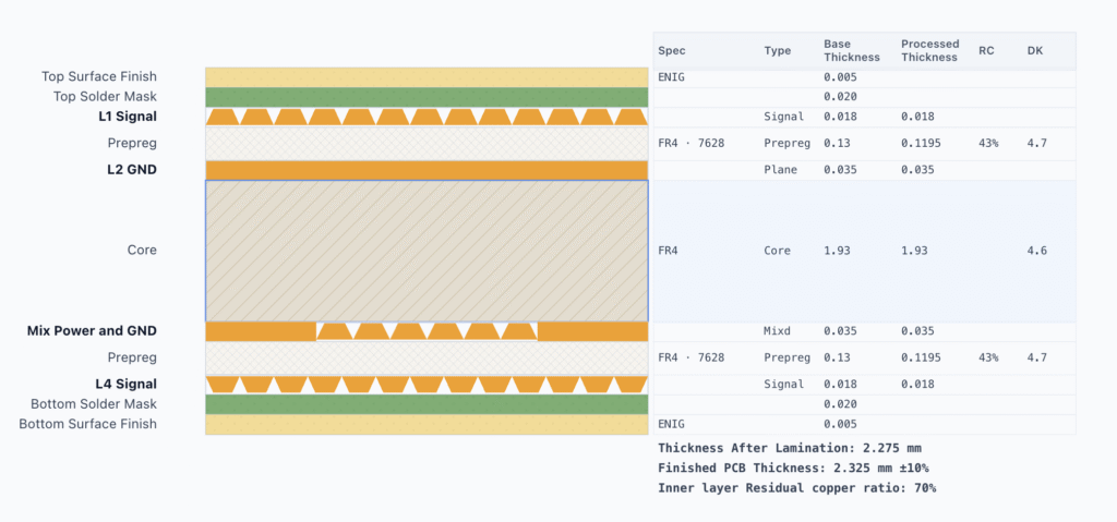
In this structure, L3 may contain power regions and local ground regions. The goal is to support L4 signals where needed while still routing power through the inner layer.
This can work for mixed-signal boards, compact industrial controls, sensor boards, and products with moderate power complexity.
But this structure can also cause serious problems when used without planning. If L3 contains many split areas, L4 signals may lose their return path. A signal routed across a plane split can create EMI and impedance issues. A mixed plane only works when the designer controls which signals route over which regions.
Use this option when you can plan L3 around the routing. Keep critical signals over ground areas.
Add stitching vias near layer transitions. Treat the mixed plane as an engineered reference structure, not a random copper layer.
Need help choosing the right 4-layer PCB stackup?
Material Choices: FR-4, Low-Loss Laminates, and Hybrid Stackups
Standard FR-4 is suitable for many 4-layer boards. Do not select a more expensive material simply because the design includes a high-speed interface. The key factors are signal length, frequency, and cost.
A short USB or Ethernet route on a small board may work well with standard FR-4. A longer high-speed route, RF path, or high-frequency module may need lower-loss material.
Low-loss laminates reduce dielectric loss at higher frequencies. They can support better insertion loss and more stable high-frequency behavior. But they cost more and may require different fabrication settings.
A hybrid dielectric stackup uses different material types in the same board. For example, a design may use a low-loss material near an RF layer and standard FR-4 elsewhere to control cost.
Using different materials in one stackup can increase manufacturing risk. These materials may have different CTE values, resin flow, and lamination requirements. Before production, you should confirm with the PCB manufacturer that all materials are compatible within the same stackup.
Hybrid 4-layer stackups work well for special designs like RF front-end modules.
They also suit antenna matching networks, high-frequency sensors, and some compact 5G edge devices. They do not make sense for most low-cost digital boards.
Via Strategy in a 4-Layer PCB Stackup
Via strategy is closely related to 4-layer PCB stackup design. The stackup defines the signal and plane layers, while vias decide how signals, power, and ground connect between those layers.
Plated through-holes are the most common and cost-effective via choice for a 4-layer PCB. For most general digital boards, through-hole vias are reliable, easy to manufacture, and low cost. The drawback is that they occupy space on all layers. Too many through-hole vias can block routing channels and reduce the continuity of internal ground or power planes.
For high-speed signals, vias also affect the return path. When a signal changes layers, its return current needs a nearby path as well. If a high-speed trace moves from one layer to another, place a ground stitching via close to the signal via. This helps the return current move between reference planes and reduces noise and EMI risk.
Small BGA packages may need blind vias or via-in-pad. A blind via from L1 to L2 can free routing space, while via-in-pad can help with fine-pitch BGA escape. These options are useful for compact modules, wearable devices, and dense IoT boards.
Blind vias usually increase PCB manufacturing cost and require more precise process control. If you use via-in-pad, you may need to fill and cap the vias, which can further increase cost and lead time.
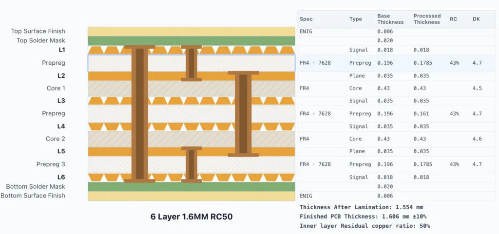
If the design needs many blind vias, high-speed interfaces, and several power rails, a 6-layer HDI stackup may work better than 4 layers. More layers can provide cleaner routing, better reference planes, and a more stable power distribution network.
Copper Weight and Prepreg Choices
Copper weight affects both routing and impedance.
A 0.5 oz starting copper layer supports finer lines and spaces more easily. A 1 oz copper layer gives stronger current capacity and remains common for many products. A 2 oz copper layer supports higher current but makes fine-line etching harder.
Copper also affects manufacturing tolerance. Thick copper needs more etching compensation. Fine traces become harder to control. If the board needs both high current and high-speed impedance, you may need to separate those needs by layer or region.
Even when two boards have the same nominal thickness, the actual spacing between signal and reference planes can differ. This is why controlled impedance designs should use the factory-confirmed stackup instead of a generic template.
This matters because dielectric thickness drives impedance. If the pressed thickness changes, the impedance changes too.
Common Mistakes in 4-Layer PCB Stackup Design
The first mistake is choosing the most common stackup instead of the right one. Signal / Ground / Power / Signal works for many boards, but it is not always the best choice for high-speed products.
The second mistake is routing high-speed signals over split planes. This can break the return path and create noise. If a trace needs a reference plane, keep that plane continuous under the trace.
The third mistake is using an online impedance calculator as the final source of truth. Calculators help during planning, but the manufacturer must confirm the final geometry based on real material and process data.
The fourth mistake is forcing a 4-layer design when the board needs 6 layers. More layers can sometimes reduce risk and save engineering time. Do not treat layer count as the only cost metric.
Conclusion
A good 4-layer PCB stackup makes routing easier, improves test results, and reduces production risk. A poor stackup can make a simple board hard to debug.
You can use our PCB Stackup Design Tool to compare common 4-layer stackup templates.
This tool also lets you define materials, adjust copper thickness, and review via. For more demanding designs, our engineers can review your stackup for manufacturability before production.
Need a reliable 4-layer PCB stackup? Get expert support before production.
FAQ
Frequently Asked Questions
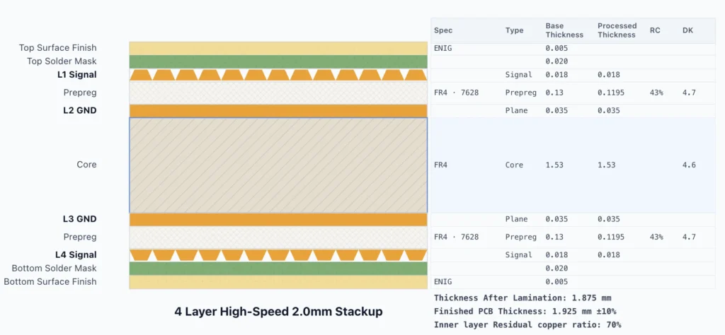
What thickness options are available for 4-layer PCBs?
HXD also supports 0.8mm, 1.2mm, 2.0mm, and 2.4mm options for different mechanical and stackup requirements.
Is Signal / Ground / Power / Signal always the best 4-layer PCB stackup?
It works well for general digital boards and designs with more power routing needs. For high-speed or EMI-sensitive boards, two ground planes may work better.
Can a 4-layer PCB support controlled impedance?
Always ask the PCB manufacturer to confirm the production stackup and final trace width.
Should I use two ground planes in a 4-layer PCB?
When should I upgrade from 4 layers to 6 layers?
Does Surface Finish Affect a 4-Layer PCB Stackup?
For normal low-speed 4-layer digital boards, the effect is small. For RF or precision impedance traces, confirm the finish with your PCB manufacturer.