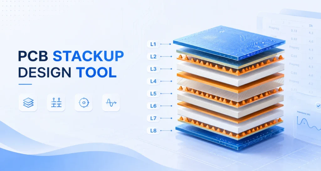
PCB Stackup Design Tool Guide
Introduction
In daily PCB stackup design, we often receive only a simple Excel stackup table from the customer. These files may show the layer order,but they often miss key stackup data. This includes resin content, prepreg type, copper thickness, dielectric constant, and final pressed thickness. As a result, checking PCB thickness and controlled impedance by hand can take time and lead to mistakes.
That is why we developed our PCB stackup design tool. It helps engineers build a clearer PCB stackup, review missing material data, and make early checks before fabrication. The goal is simple: turn incomplete Excel stackup data into a more visual, useful, and manufacturable stackup plan.
In this guide, we explain key PCB stackup parameters to know before design. These include materials, copper thickness, dielectric layers, and impedance data. We will also show how to use the tool step by step, so you can create, check, and adjust a PCB stackup more efficiently.
Different types of layers in a stack-up
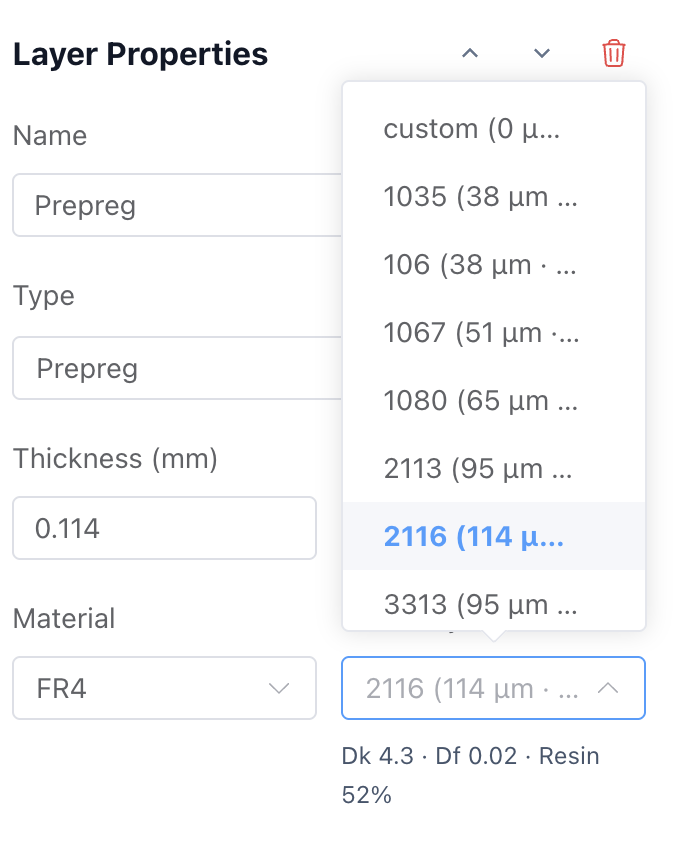
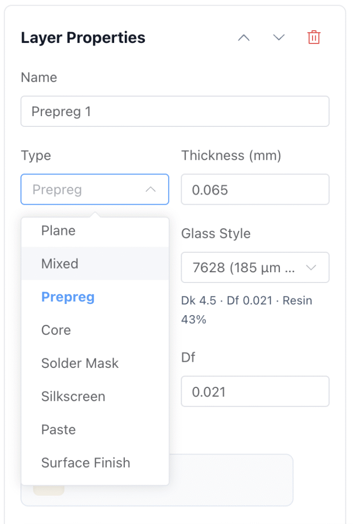
Prepreg
Prepreg works as both a bonding layer and an insulating layer in a multilayer PCB.
In a multilayer PCB, manufacturers usually place prepreg between copper layers or between core layers. During lamination, heat softens the resin inside the prepreg. The resin flows and bonds the nearby layers together. After it cools and cures, it forms a stable insulating layer between the copper layers.
Common Types of PCB Prepreg
| Grade | Typical Marking |
| Low Resin Content(SR) | 7628L, 2116SR |
| Medium Resin Content(MR) | 7628M, 2116MR |
| High Resin Content(HR) | 7628H, 1080HR |
Our tool includes common PCB prepreg glass styles, making it easier to choose the right prepreg for your stackup.
PCB Glass Styles Explained
| Glass Style | Nominal Thickness (mm) | Typical Resin Content | Typical Dk — FR-4 System (1 GHz) |
| 106 | 0.038 | 70–78% | 3.7–4.0 |
| 1035 | 0.025–0.028 | 63–70% | 3.6–3.9 |
| 1067 | 0.032 | 62–66% | 3.7–4.0 |
| 1078 | 0.040–0.050 | 57–68% | 3.6–3.9 |
| 1080 | 0.064 | 58–72% | 3.8–4.2 |
| 1086 | 0.050 | 58–67% | 3.7–4.1 |
| 2313 | 0.080 | 52–58% | 3.9–4.3 |
| 3313 | 0.081 | 50–58% | 3.9–4.3 |
| 2116 | 0.097 | 48–62% | 4.0–4.5 |
| 1501 | 0.140 | 43–47% | 4.3–4.6 |
| 1506 | 0.140 | 43–47% | 4.3–4.6 |
| 1652 | 0.114 | 47–52% | 4.2–4.5 |
| 7628 | 0.173 | 40–52% | 4.3–4.8 |
2116 is one of the most commonly used prepreg glass styles in the PCB industry. It often used as the go-to option for standard 4- to 8-layer PCBs. Most PCB factories keep it in stock, which helps control cost and lead time.
Notes:
- Different material suppliers (Isola, Panasonic, Ventec, Shengyi, etc.) may show ±0.1–0.3 variation in Dk because of different resin formulations.
- Resin Content (RC) shows typical ranges; values vary by SR/MR/HR grade within the same style.
- Dk values are typical for standard FR-4 systems measured at 1 GHz.
- Dk decreases slightly with higher resin content and at higher frequencies.
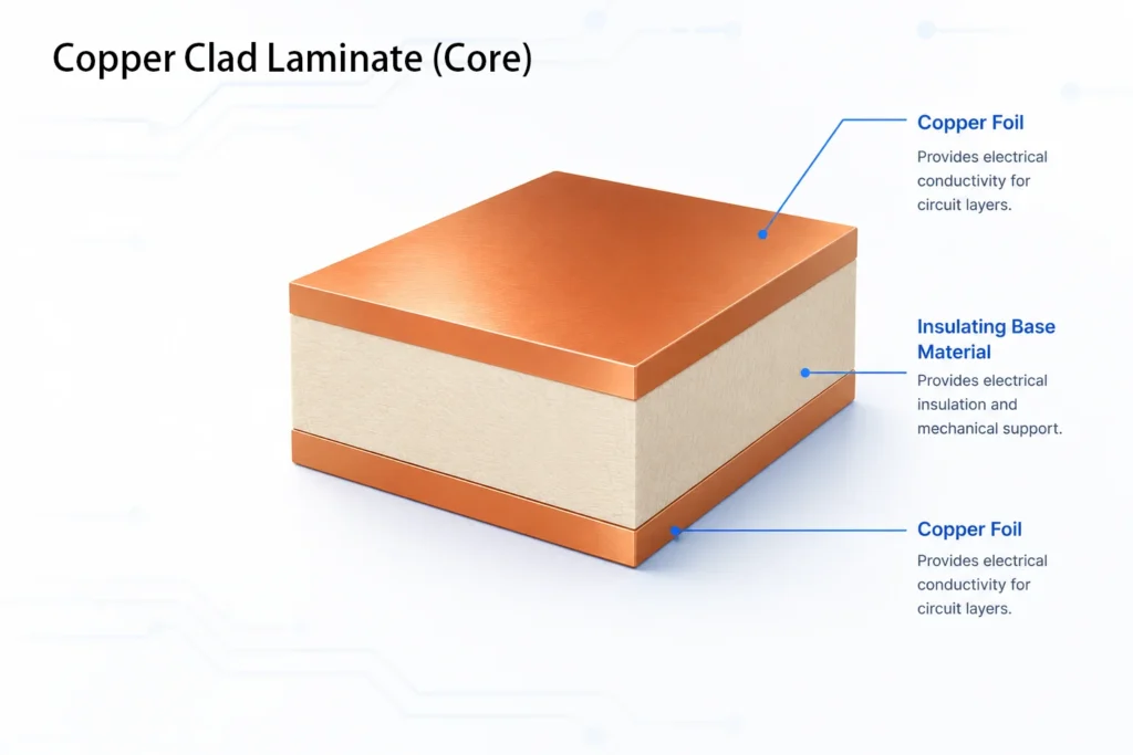
Core
Core(Copper Clad Laminate) is a rigid base layer used in a multilayer PCB. It is made of an insulating base material with copper foil bonded to one or both sides. The core has stable thickness and strong mechanical support.
A basic PCB core structure looks like this:
The insulating base material can be different depending on the PCB application. Common materials include FR-4, High-Tg FR-4, Rogers, PTFE, and Polyimide.
When selecting a PCB core, check these key points:
- Heat resistance: Check values such as T288, and T300. These show how well the material can handle heat.
- Strength: The laminate should have enough bending strength and peel strength for the product.
- Size stability: The material should stay stable during PCB manufacturing and soldering.
- Chemical resistance: The laminate should resist chemicals used in production and harsh working conditions.
- Tg: The glass transition temperature should match the working temperature of the PCB.
- Dk and Df: For high-speed PCBs, lower Dk and Df values help reduce signal loss.
- Moisture resistance: Low water absorption is important for boards used in humid or harsh environments.
You can use our PCB Material Selector to find the right material.
Signal layers
Signal layers are PCB copper layers used to route electrical signals between components. They carry traces for data, clocks, RF, and control lines. In a good stackup, signal layers stay close to ground planes to reduce noise and improve signal integrity.
Power and ground layers
Power and ground layers are large copper planes in a PCB. Power layers deliver stable voltage to components, while ground layers provide return paths for signals. They reduce voltage drop, lower noise, improve power integrity, and help shield signal layers from EMI.
Soldermask
Soldermask is a protective coating applied over the PCB surface. It covers copper traces to prevent oxidation, scratches, and solder bridges. It leaves pads, holes, and test points exposed for soldering. Soldermask also improves assembly quality and helps keep nearby copper features electrically isolated.
Silkscreen layers
Silkscreen layers are printed marking layers on a PCB surface. They show component names, polarity marks, logos, version numbers, and assembly notes. Silkscreen does not conduct electricity. It helps engineers identify board information quickly.
Paste layer
Paste in a PCB stackup usually means the solder paste layer. It defines where solder paste is printed on surface-mount pads through a stencil before SMT assembly. Paste layers do not conduct electricity and are not physical stackup layers. They help control solder volume and assembly quality.
Copper thickness
Common copper thickness can range from 0.5oz to 3oz, based on your application. Copper weight affects current, heat, trace size, impedance, and cost.
Layer arrangement guidelines for a PCB
1.Add interleaved ground planes
Ground planes are the backbone of a stable PCB stackup. They provide a low-impedance return path for signals and help reduce EMI.
If the reference plane is missing, split, or too far away, the return current may take a longer path.
For high-speed PCB designs, place signal layers close to ground planes whenever possible. This reduces the return loop area and helps control noise, crosstalk, and EMI. A smaller loop means less radiation, less noise pickup, and better signal quality.
2. Use multiple power planes
A power plane is a large copper area used to distribute voltage across the PCB.
Using multiple power planes can help separate noisy and sensitive power domains. This is important in mixed-signal boards, RF boards, high-speed digital boards, and power electronics.
3. Avoid placing adjacent signal layers
Adjacent signal layers can cause crosstalk and EMI issues. This is worse without a solid reference plane between them.
When two signal layers sit next to each other, electric and magnetic fields from one layer can couple into the other. This is worse when the traces run in the same direction.
4. Try not to add splits in the power plane
Power plane splits can create signal integrity problems when signals use the power plane as a reference.
A split is a gap or division in a plane. It may be used to separate different voltage areas. That can be useful for power planning. But if a high-speed signal crosses that split, its return current may not have a direct path.
5. Place ground planes next to power planes
Power and ground planes should be placed close together when possible. This improves power integrity and helps lower noise.
In PCB stackup design, placing a power plane close to a ground plane creates a plane pair. This structure helps improve power integrity, reduce noise, and support better EMI performance. This plane pair can reduce loop inductance and help the power distribution network behave better at high frequency.
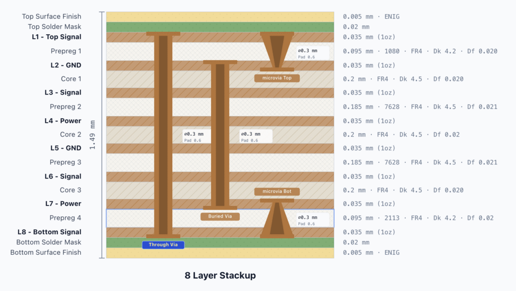
HDI stack-ups
HDI boards can fit more traces in the same PCB area than traditional PCBs. They use buried vias, blind vias, and microvias to create shorter connections and better electrical performance.
An HDI stackup combines power layers, ground layers, and signal layers in one compact structure. With multiple layers, engineers can build smaller boards for modern products with complex circuits. This structure also provides more routing space for component connections.
However, HDI stackups require a more complex manufacturing process.
Standard multilayer PCBs usually use mechanical drilling and one-time lamination.
HDI PCBs often use laser microvias, multiple lamination cycles, and high-density routing.
An HDI PCB may require the following process:
- Inner core fabrication
- First lamination
- Laser drilling
- Copper plating and via filling
- Second lamination
- Laser drilling again
- Copper plating again
- Outer layer fabrication
For 2+N+2 or 3+N+3 HDI structures, the number of lamination cycles will continue to increase.
Different types of HDI stack-ups
The X+N+X structure in HDI PCB refers to HDI build-up layers added to both sides of a standard multilayer core. N is the core layer count, and X is the number of build-up layers on each side. A higher X value allows higher routing density and more advanced microvia structures, but it also increases lamination cycles. It also increases manufacturing complexity and cost.
IPC-2226 groups HDI PCB stackups into several structure types. Most designs use Type I, Type II, and Type III.
Type I uses one microvia layer and no buried vias.
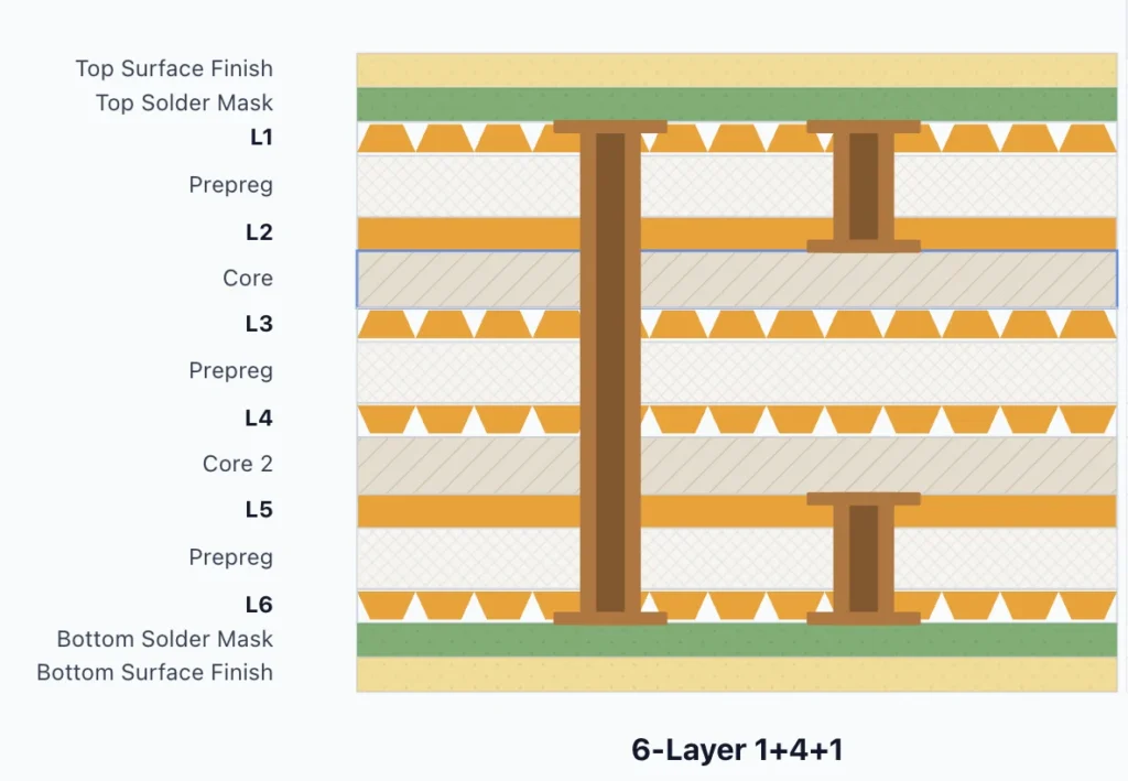
Type II adds buried vias in the core.
Type III uses two or more microvia build-up layers.
Examples include 2+N+2 or 3+N+3 structures. More advanced Type V and Type VI designs often link to ELIC or any-layer HDI.
Conclusion
A clear PCB stackup helps reduce design errors, improve signal performance, and make fabrication communication easier. With the PCB Stackup Design Tool, you can visualize layer structures, and prepare better stackup data before production. If you have better suggestions, please contact us.
Need help turning stackup data into a manufacturable PCB design? Try our PCB Stackup Design Tool or contact our engineering team for a stackup review.