Rogers 4003C PCB Manufacturing Guide
Think Deeper with AI:
Introduction
Rogers 4003C is widely used in RF, microwave, radar, and high-speed PCB designs.
This guide explains RO4003C from a practical production view. It covers material properties, stackup design, hybrid construction, fabrication limits, and sourcing decisions.
The goal is to help engineers and buyers decide when Rogers 4003C is the right PCB material.
Rogers 4003C Datasheet Overview
Rogers 4003C offers stable Dk, low Df, and good thermal reliability. Its datasheet values help engineers evaluate impedance, signal loss, stackup design, and high-frequency PCB performance.
| Parameter | Value | Notes |
|---|---|---|
| Material Type | Hydrocarbon ceramic / woven glass laminate | Non-PTFE high-frequency laminate |
| Process Dk | 3.38 ± 0.05 | Measured at 10 GHz / 23°C |
| Design Dk | 3.55 | Used for microstrip and stripline impedance design |
| Dissipation Factor / Df | 0.0027 | Measured at 10 GHz / 23°C |
| Df at 2.5 GHz | 0.0021 | Reference value at a lower frequency point |
| Thermal Coefficient of Dk | +40 ppm/°C | Measured from -50°C to 150°C |
| Z-axis CTE | 46 ppm/°C | Measured from -55°C to 288°C |
| X-axis CTE | 11 ppm/°C | Measured from -55°C to 288°C |
| Y-axis CTE | 14 ppm/°C | Measured from -55°C to 288°C |
| Glass Transition Temperature / Tg | >280°C | Measured by TMA |
| Decomposition Temperature / Td | 425°C | Measured by TGA |
| Thermal Conductivity | 0.71 W/m·K | Measured at 80°C |
| Moisture Absorption | 0.06% | Measured after 48-hour immersion |
| Density | 1.79 g/cm³ | Measured at 23°C |
| Copper Peel Strength | 1.05 N/mm / 6.0 pli | Based on 1 oz ED copper |
| Volume Resistivity | 1.7 × 10¹⁰ MΩ·cm | Condition A |
| Surface Resistivity | 4.2 × 10⁹ MΩ | Condition A |
| Electrical Strength | 31.2 kV/mm / 780 V/mil | Based on a 0.51 mm sample |
| Flammability | N/A / Non-FR | RO4003C is not UL 94 V-0 rated |
| Lead-Free Process Compatibility | Yes | Compatible with lead-free PCB assembly |
| Common Thicknesses | 0.008”, 0.012”, 0.016”, 0.020”, 0.032”, 0.060” | Equivalent to 0.203–1.524 mm |
| Copper Cladding | 0.5 oz, 1 oz, 2 oz ED copper | LoPro foil options are available |
For more RO4003C material details, you can check our PCB Material Selector.
Process Dk vs Design Dk
Rogers 4003C has two dielectric constant values that designers should understand: Process Dk and Design Dk. They serve different purposes, so you should not treat them as the same value.
Process Dk is the material test value measured under a defined test method. For RO4003C, the typical Process Dk is 3.38 ± 0.05 at 10 GHz and 23°C. This value is useful when comparing laminate materials, checking incoming material quality, or reviewing datasheet specifications.
Design Dk is the value used for practical transmission line design.
For impedance calculation, engineers should use Design Dk, not only the datasheet Process Dk. Using Process Dk directly may cause impedance deviation, especially in controlled impedance RF boards. Trace width, dielectric thickness, copper thickness, solder mask, and fabrication tolerance also affect the final impedance.
In production, confirm Ro4003C impedance with the PCB manufacturer before fabrication. For critical RF designs, use test coupons and TDR measurements.
RO4003C PCB Cost Factors
The cost of an RO4003C PCB is not determined by laminate price alone. Several design and manufacturing factors can affect the final quotation.
Main cost drivers include:
- Laminate thickness
- Copper weight
- Total layer count
- Hybrid stackup or full Rogers stackup
- Controlled impedance requirements
- Surface finish selection
- Tight etching tolerance
- RF testing or impedance testing requirements
- Material availability and lead time
A full RO4003C stackup usually costs more than a hybrid structure. In many RF boards, designers use RO4003C only on critical signal layers and use FR4 in non-critical layers.
Controlled impedance, fine trace spacing, heavy copper, and advanced testing can also increase production cost. For this reason, review the stackup with the PCB manufacturer before the final layout.
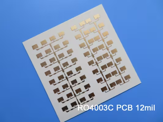
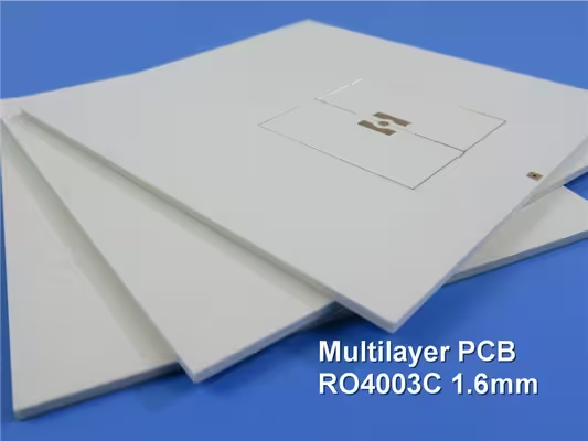
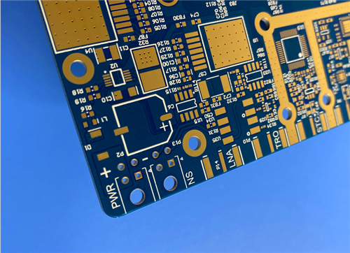
Rogers 4003C PCB Products
Below are our Rogers 4003C PCB products, including different stackups, thicknesses, surface finishes, and application examples.
Want to learn more about Rogers 4003C PCB options? Contact us to discuss your stackup, and manufacturing requirements.
RO4003C PCB Cost Factors
The cost of an RO4003C PCB is not determined by laminate price alone. Several design and manufacturing factors can affect the final quotation.
Main cost drivers include:
- Laminate thickness
- Copper weight
- Total layer count
- Hybrid stackup or full Rogers stackup
- Controlled impedance requirements
- Surface finish selection
- Tight etching tolerance
- RF testing or impedance testing requirements
- Material availability and lead time
A full RO4003C stackup usually costs more than a hybrid structure. In many RF boards, designers use RO4003C only on critical signal layers and use FR4 in non-critical layers.
Controlled impedance, fine trace spacing, heavy copper, and advanced testing can also increase production cost. For this reason, review the stackup with the PCB manufacturer before the final layout.
FAQ