


HXDcircuit

What is ENIG?

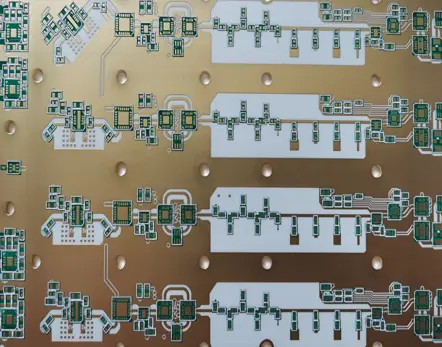
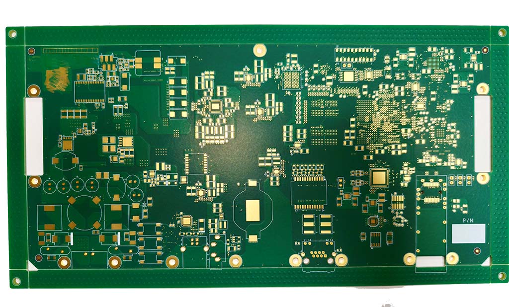
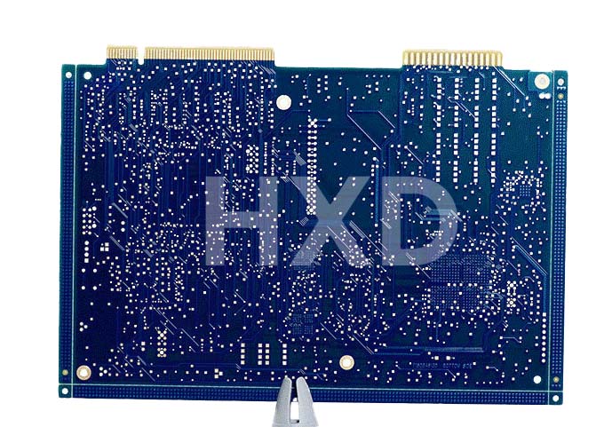
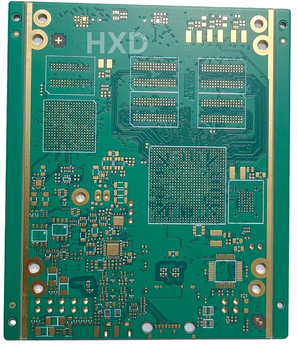
HXD ENIG PROCESS PCB

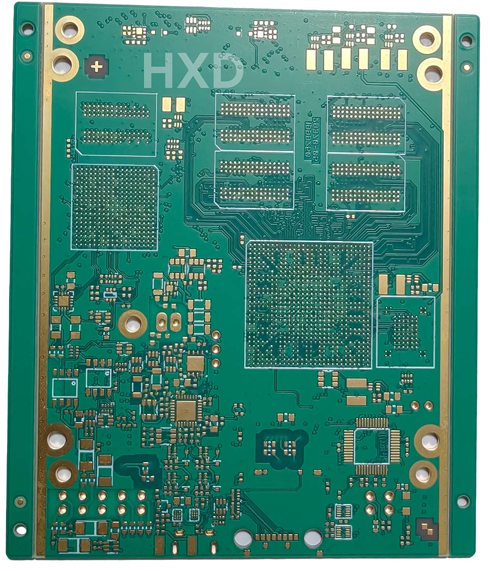
ENIG (Electroless Nickel Immersion Gold)is a common PCB surface finish.  It is created by depositing a layer of nickel-phosphorus (Ni-P) onto the bare copper, followed by a thin layer of immersion gold.

This combination protects the copper and improves solderability. It is designed to meet modern requirements for reliability, surface flatness, and environmental compliance.

ENIG strictly limits the use of harmful substances like lead, mercury, and cadmium in electronic products. It is a RoHS-compliant surface finish.

PCB Certifications

HXD ENIG Process

12Layer FR4 ISOLA 370HR Tg170

12Layer FR4 ISOLA 370HR Tg170

Reliable Supply of ISOLA 370HR (Tg170),Industrial-Grade 12-Layer Stack-Up,High-Precision Conductive Performance

12Layer HDI with ISOLA 370HR Tg170

12Layer HDI with ISOLA 370HR Tg170

12-layer stackup with multiple HDI build-up (L1-2, L11-12) enables high-density routing, compact layouts, and advanced miniaturized designs.

14Layer with FR4 Tg180

14Layer with FR4 Tg180

Designed for complex, high-speed broadcasting systems requiring multi-layer signal integrity and stable performance.

8-Layer FR4 Tg170 PCB

8-Layer FR4 Tg170 PCB

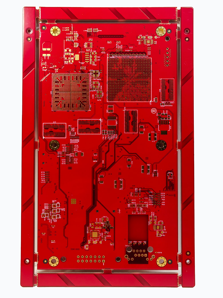
Material: Fr4 Tg170 Board Thickness: 2.0mm Surface Finish: ENIG Certificated: ISO9001 ISO14001 UL

Get started with your next project

Upload your Gerber files to get an instant quote.

Start Custom Quote

HXD ENIG Quality Assurance

​​Black Pad is the most common quality defect in the ENIG process. It appears as a dark, corroded area on the nickel surface beneath the gold layer. To prevent this, we implement strict process controls:

pH Monitoring: We monitor the pH levels of the nickel bath in real-time. This is critical because the pH level directly reflects the phosphorus content in the solution.

Reaction Control: We maintain the gold-to-nickel displacement reaction within ideal parameters to ensure a smooth, healthy bond.

EPIG Alternative: For projects requiring even higher reliability, we offer EPIG (Electroless Palladium Immersion Gold). This process uses a palladium layer to completely eliminate nickel-related “Black Pad” risks at the source.

HXD ENIG Thickness Standards

HXD’s ENIG process fully complies with the IPC-4552 standard:

Nickel Layer: 2.54 to 6.35 µm (100–250 µin)

Gold Layer: 0.05 to 0.2 µm (2–8 µin)

Key Benefits of ENIG

Excellent Flatness

The gold layer in ENIG is extremely uniform, creating a nearly perfectly flat surface. This flatness is critical for BGA, QFN, and fine-pitch components. it ensures precise placement and significantly reduces soldering defects.

Longer Shelf Life

Gold is naturally resistant to oxidation. It acts as a shield, protecting the underlying nickel and copper from air corrosion. This gives the boards a longer shelf life—typically 12 months or more.

Superior Solderability

The ENIG surface structure promotes excellent solder wetting and spreading. This makes the soldering process more stable and reliable during assembly.

Keypad Applications

Due to its high reliability and conductivity, ENIG is a top choice for keypad circuits that must withstand thousands of presses. Unlike Hard Gold, ENIG pads are both wear-resistant and solderable. This allows buttons or other components to be soldered directly onto the same pads used for the contact interface.

REQUEST A QUOTE

Supported file formats: PDF, DOC, DOCX, TXT, JPG, PNG (Max 2MB)