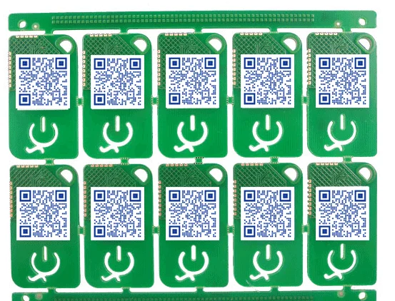
How to Tell How Many Layers a PCB Has
 steve ran
August 23, 2026
steve ran
August 23, 2026
The most reliable way is to check the PCB stackup or fabrication data. These records identify every copper layer and show the physical order of the board.
What Counts as a Layer in a PCB?
A PCB layer count refers to the number of conductive copper layers in the board. A 4-layer PCB, for example, contains four copper layers separated by insulating materials.
We’ll use a typical 4-layer PCB stackup as an example to explain the PCB layer structure.
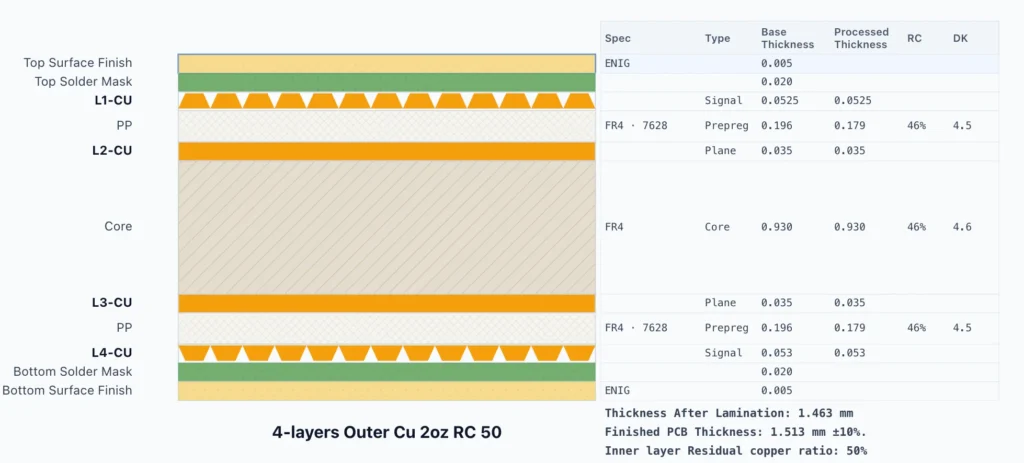
A typical 4-layer PCB stackup includes the following layers:
- Top Signal Layer: The outer copper layer on the primary component side. It contains component pads, traces, and copper areas for routing signals and local power connections.
- Ground Plane: A continuous internal copper layer connected to ground. It provides short return paths, reduces EMI, and improves signal integrity.
- Power Plane: An internal copper layer that distributes supply voltages across the board. It provides a low-impedance power path and supports stable power delivery to components.
- Bottom Signal Layer: The outer copper layer on the opposite side. Designers use it for extra routing, component pads, and copper pours when the top layer has limited space.
A PCB contains many material and documentation layers that do not conduct signals. These do not increase the stated PCB layer count.
What Doesn’t Count as a PCB Layer?
Core and Prepreg form part of the physical stackup, but manufacturers do not count them as conductive PCB layers. The same rule applies to solder mask, silkscreen, paste, and mechanical data. The following sections explain the purpose of each of these layers.
Core: A cured laminate that provides mechanical strength and electrical insulation between copper layers.
Prepreg: A resin-coated fiberglass material that bonds the PCB layers during lamination and controls dielectric spacing.
Solder Mask: A protective coating that covers outer copper, prevents oxidation, and reduces solder bridging.
Silkscreen: Silkscreen is a printed layer that shows component labels, polarity marks, symbols, and assembly information.
Paste Layer: A production file that defines where a stencil should deposit solder paste on surface-mount pads.
Mechanical Data: Documentation that defines the board outline, cutouts, dimensions, slots, and other fabrication details.
What Is the Most Reliable Way to Identify PCB Layer Count?
No single inspection method suits every situation. The right choice depends on the available records, and required accuracy.
Use the methods in this order:
- Review the stackup drawing and fabrication data.
- Analyze vias and visible routing clues.
- Use X-ray or CT inspection.
- Prepare a microsection when you need final physical confirmation.
Review the Stackup Drawing
The stackup drawing provides the clearest answer when controlled manufacturing records remain available. It shows the copper layers in physical order. It often includes their functions, copper weights, dielectric materials, and finished thicknesses.
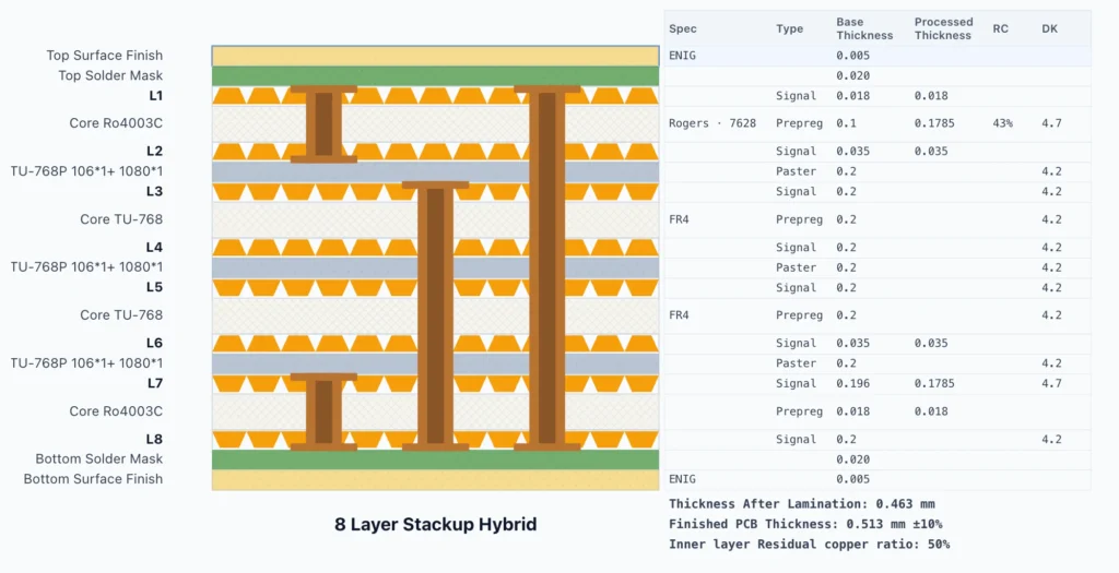
This stackup illustrates HXD’s typical 8-layer PCB structure. An 8-layer PCB consists of eight copper layers.
Gerber files can show the copper layers, but they do not include the complete PCB stackup or material information. The IPC-2581 Consortium notes that Gerber transfers image data but does not transfer stackup and material data by itself.
ODB++ usually provides clearer layer identification because the data structure records layer assignments. Altium’s fabrication-data documentation explains that ODB++ stores layer identification in its matrix file. However, engineers should still confirm the physical order after importing the data.
Analyze Vias and Visible Routing Clues
If the manufacturing files are not available, the PCB itself may provide useful clues. Vias, routing patterns, and component density can reveal whether the board contains internal copper layers.
Through-Hole Vias
A plated through-hole via extends from the top surface to the bottom surface. It may connect to one or more inner layers.
But you cannot tell how many inner layers it has just by looking at the outside. A board with many through-hole vias could have two, four, six, or more layers. Through vias alone cannot confirm the total PCB layer count.
Blind and Buried Vias
A blind via connects an outer copper layer to one or more internal layers without passing through the full board. A buried via connects internal layers and does not reach either outer surface.
Finding a blind or buried via confirms that the PCB contains internal conductive layers. However, the via still may not reveal the exact total.
For example, a blind via that connects L1 to L2 proves that L2 exists. It does not prove whether the board has four, six, eight, or more copper layers.
Visible Routing Clues
Surface routing can provide additional evidence. A trace may enter a via, disappear from the visible surface, and connect to another location. This pattern suggests routing through an internal layer.
Other possible clues include:
- Dense BGA breakout routing
- High component density
- Few visible surface traces
- Large areas without visible power routing
- Signals entering vias without visible surface connections
Complex BGA routing often requires internal signal and reference layers. Still, board designers can use different routing strategies, microvias, or fine traces. Density indicates possible complexity, not an exact layer count.
Use these features to determine whether a board is likely multilayer. Do not use them as final proof that a PCB has a specific number of layers.
Use X-Ray or CT Inspection
X-ray inspection provides a non-destructive way to examine hidden features inside a PCB. Copper absorbs X-rays differently than the surrounding resin and glass-reinforced dielectric. This lets inspection equipment reveal internal traces, planes, vias, and plated holes.
X-ray works well when:
- The original manufacturing files are missing.
- The PCB must remain functional.
- Visual inspection cannot reveal the internal construction.
- An engineer needs to investigate internal routing or defects.
- A quality team needs evidence for failure analysis.
However, a standard two-dimensional X-ray image compresses the board’s internal structures into a single projection. Copper patterns from several layers may overlap. Dense components, solder joints, shields, and large copper planes may also hide fine features.
You can change the viewing angle to improve visibility. For more complex PCBs, we use CT or laminography to inspect the internal structure.
X-ray or CT offers the best option when the board must remain intact. However, complex structures may still require physical sectioning for final confirmation.
Use Microsection Analyze for Final Confirmation
Microsection examines provides direct physical evidence of a PCB’s internal construction. A small PCB sample is embedded in resin, polished, and examined under a microscope.
According to IPC-TM-650, microsection analysis measures copper thickness, dielectric spacing, plating thickness, and layer alignment.
Need a Professional PCB Stackup Design?
Optimize your PCB performance with a professionally designed stackup. Our engineers can help you select the right layer structure, materials, and impedance requirements for your project.
Get StartedConclusion
The best way to tell how many layers a PCB has is to review the correct stackup drawing or manufacturing data. These records identify the copper layers and show their physical order.
Gerber files can reveal copper artwork layers, but they may not define the full physical stackup. ODB++ and IPC-2581 data often carry more structured layer information.
Vias and visible routing provide useful clues when files are missing. Blind and buried vias confirm internal connections, but they do not always reveal the exact number of copper layers.
X-ray and CT inspection offer non-destructive ways to examine internal PCB structures. Microsection analysis provides final physical confirmation and can also measure copper thickness, dielectric spacing, hole plating, and layer alignment.