


HXDcircuit

What is HASL?

hasl surface finish

HASL (Hot Air Solder Leveling) is a common and mature PCB surface finish process. Its main purpose is to form a solderable and oxidation-resistant solder layer on copper pads, making component assembly easier and more reliable.

Typical HASL Process Flow:

  1. Pre-cleaning The PCB is cleaned to remove oil, oxides, and contaminants. This ensures a clean copper surface and improves solder wetting.
  2. Preheating The board is heated evenly. This reduces thermal shock when it enters the hot solder bath and helps the flux work more effectively.
  3. Flux Coating Flux is applied to the PCB surface. It removes remaining oxides and lowers surface tension to improve solder quality.
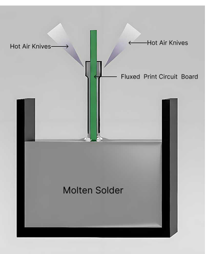
  4. Solder Coating The PCB is dipped into a bath of molten solder (leaded or lead-free). This covers all exposed copper pads and holes with solder.
  5. Air Knife Leveling As the PCB leaves the solder bath, high-pressure hot air (air knives) blows away extra solder. This makes the solder thickness on the pads more even.
  6. Post-cleaning After the solder cools and hardens, the PCB is cleaned again. This removes flux residues to ensure the board is clean and reliable.

PCB Certifications

HASL Process PCB

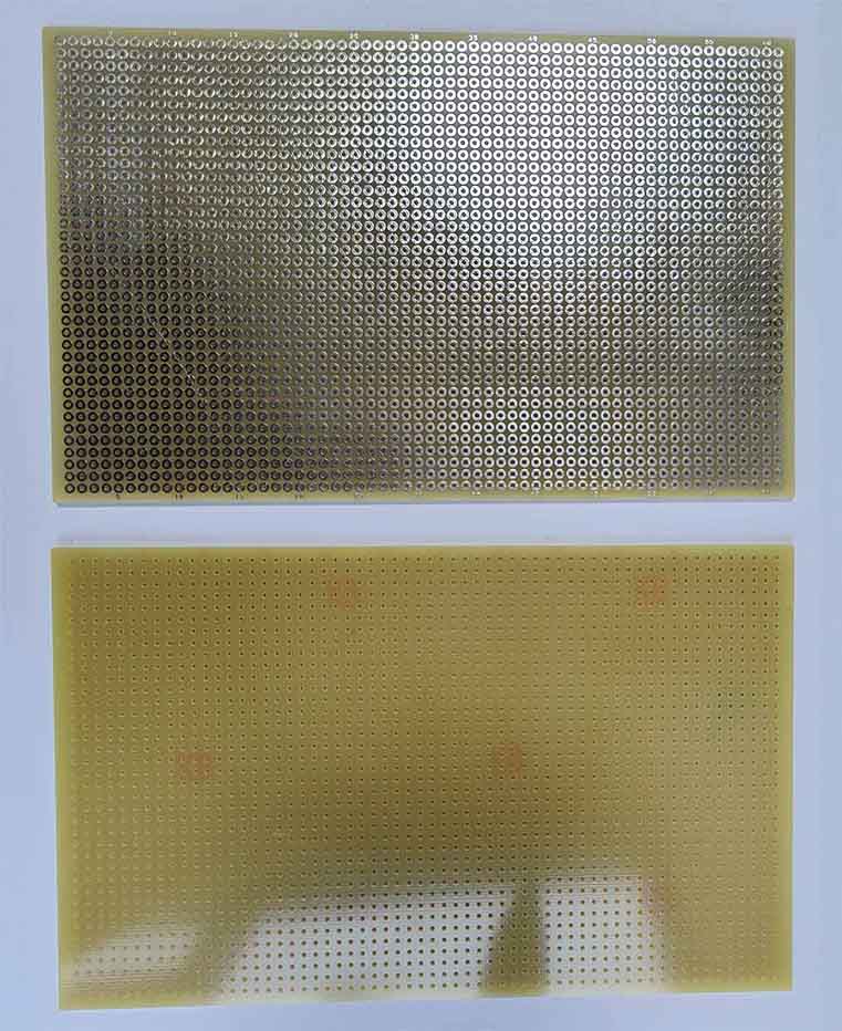
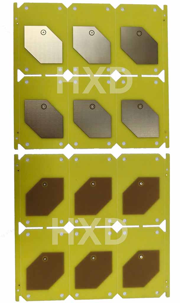
1Layer with HASL LF

1Layer with HASL LF

FR4 Material with HASL LF– Cost-effective and ideal for beginner projects, quick prototyping, training, and educational use. HASL LF has excellent solderability for repeated testing and manual solder experiments.

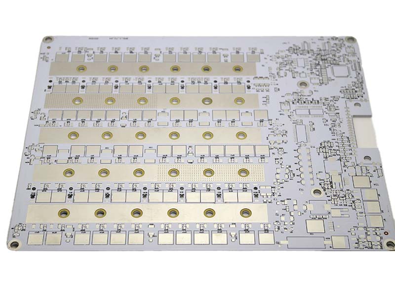
2Layer Aluminum PCB

2Layer Aluminum PCB

Offers improved routing flexibility and electrical performance compared to standard single-layer MCPCBs—ideal for more complex lighting designs.

2Layer with 0.6mm thin thickness

2Layer with 0.6mm thin thickness

Better Flexibility Than Standard Thickness – Slight bending tolerance makes it suitable for tight assembly structures.

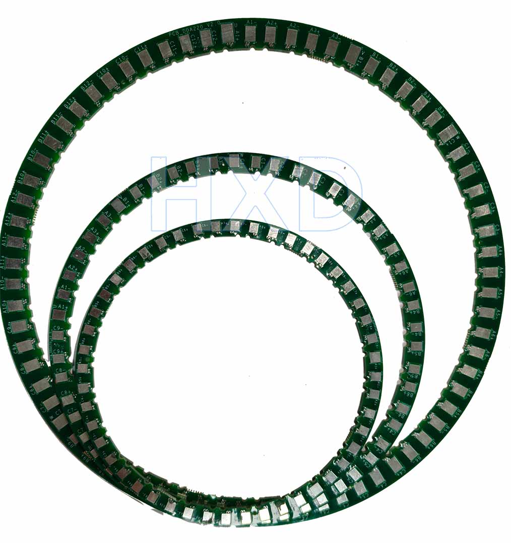
6Layer roud PCB with long routing

6Layer roud PCB with long routing

Our 6-layer round PCB combines a complex circular shape with high-density 4/4mil track

Need a Reliable HASL PCB Solution?

Get high-quality HASL surface finish PCBs with stable performance. Contact our engineering team for a custom quote today.

Start Custom Quote

HASL Advantages & Limitations

HASL is a low-cost PCB surface finish with good solderability. It is widely used in standard PCB and LED lighting production. However, it has poor surface flatness and is not suitable for high-density or fine-pitch designs.

Advantages

  • Lowest-cost PCB surface finish option

  • Excellent solderability and reliable assembly performance

  • Long storage life and good shelf stability

  • Easy rework and repair during production

Limitations

  • Poor surface flatness, not suitable for BGA or fine-pitch components

  • Leaded versions may not meet RoHS environmental requirements

  • Thermal stress may cause warping in thin PCBs

  • Not suitable for  for high-density or high-frequency designs

If you want to learn more about PCB surface finishes such as OSP, Immersion Silver, and Immersion Tin, please see here for detailed information and comparisons to help you choose the right option for your project.

Leaded HASL vs Lead-free HASL

Whether using leaded or lead-free solder, the HASL process follows the same principle. The main differences are in chemical composition, environmental compliance, and processing temperature requirements.

Features Leaded Lead-Free
Alloy Composition 63% Sn / 37% Pb 99.3% Sn / 0.6% Cu
RoHS Non-compliant Compliant
Melting Point Lower Higher

Lead-free HASL uses alloys with a higher melting point than traditional leaded solder. The process requires higher temperatures, so the PCB must withstand extra thermal stress.

We recommend high-temperature laminates (high-Tg materials) for lead-free HASL to prevent warping or damage during production.

Although lead-free HASL offers better surface flatness, it is not suitable for very small SMD components (0805 and below) or fine-pitch designs.

REQUEST A QUOTE

Supported file formats: PDF, DOC, DOCX, TXT, JPG, PNG (Max 2MB)