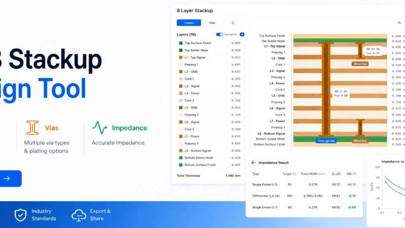
4-Layer vs. 6-Layer PCB: Stackup, Performance, and Cost
 steve ran
August 24, 2026
steve ran
August 24, 2026
A 4-layer PCB is often the right choice for designs with moderate routing density. A 6-layer PCB is a better choice when routing is tight, or when signal and power integrity needs are higher.
A 6-layer PCB is not automatically better than a 4-layer PCB. The right choice depends on the design. A well-designed 4-layer PCB can provide strong signal integrity, EMC performance, and routing. A poorly designed 6-layer PCB can still have layout issues.
This guide compares 4-layer and 6-layer PCBs to help you choose the right layer count for your design.
What Is a Typical 4-Layer PCB Stackup?
A 4-layer PCB has four conductive copper layers. Two are usually outer signal layers, while the two inner layers provide reference planes, power distribution, or both.
No single 4-layer stackup works best for every board. These two arrangements are common starting points.
Signal–Ground–Ground–Signal
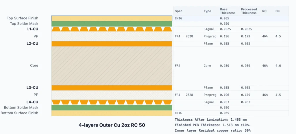
This arrangement places each outer signal layer next to a ground plane. That gives high-speed traces a nearby, continuous return path and makes controlled-impedance routing easier to define. Power must usually travel through traces, copper pours, or local power regions rather than a dedicated power plane.
This stackup can work well when the board has only a few supply rails and enough surface area for power distribution. It also provides a strong foundation for signal integrity and EMI control.
Signal–Ground–Power–Signal
This arrangement provides dedicated space for ground and power distribution. It can simplify a board with one main supply or a few well-planned power regions.
What Is a Typical 6-Layer PCB Stackup?
A 6-layer board adds two conductive layers. Designers can use that space for more routing, additional reference planes, or more organized power distribution.
One common stackup is:
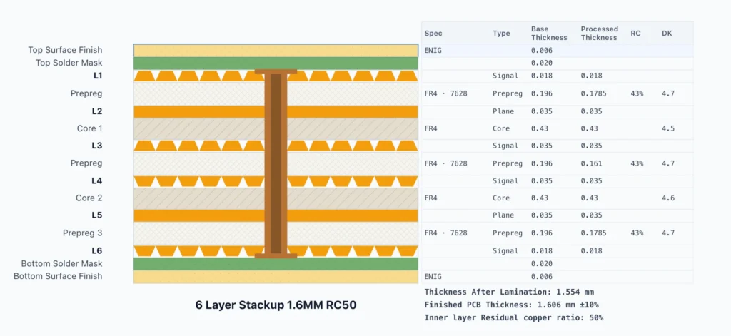
In this example, the top layer references Layer 2, the inner signal layer also has Layer 2 as a nearby reference, and the bottom layer references Layer 5. The two ground planes improve routing flexibility and provide reference options on both sides of the board.
Layer 4 can distribute one supply, contain several power regions, or support broader power routing. Any split must be planned so that high-speed signals do not cross a gap in their reference plane.
4-Layer vs. 6-Layer PCB Performance
Signal Integrity
Both 4-layer and 6-layer designs should follow these principles:
- Route fast signals next to a continuous reference plane.
- Keep the return path short and uninterrupted.
- Do not route a high-speed trace across a plane split or large void.
- Use the PCB manufacturer’s impedance geometry for controlled-impedance traces.
- Keep differential-pair geometry consistent with the interface requirements.
- Reduce unnecessary via transitions and long via stubs.
- Add nearby ground stitching vias when a signal changes between layers that use different ground reference planes.
- Control spacing between long, parallel routes to reduce crosstalk.
A 6-layer board can make these rules easier to follow because it provides more routing space and reference-plane choices.
EMI and EMC
A 6-layer PCB provides more flexibility for ground planes and separating noisy and sensitive circuits. Internal signal layers between reference planes also help improve electromagnetic field containment.
However, adding layers does not automatically solve EMI problems. Poor return paths, connector placement, long current loops, inadequate filtering, and incorrect decoupling can still cause EMI issues.
You can achieve good EMC performance on a 4-layer PCB. A continuous ground plane is more important than simply labeling a layer as ground.
Power Integrity
A 6-layer PCB gives the designer more copper area for multiple supply rails. It can also provide closer power-ground plane spacing if the manufacturer can build the required stackup. Close plane spacing increases interplane capacitance, but it does not eliminate the need for discrete decoupling capacitors.
On a 4-layer board, power may use a dedicated plane, or wider traces. This works well when current paths remain short and you meet voltage-drop targets. You should check transient current paths, regulator placement, and the impedance of the power distribution network.
For either layer count, place local decoupling close to the device power pins and connect it with short, low-inductance paths. A solid plane structure, correct decoupling, and short current loops work together. No single feature solves power integrity alone.
Thermal Performance
A 6-layer PCB can improve heat spreading, especially when internal planes are connected to thermal vias.
Layer count alone does not predict board temperature. Thermal results also depend on:
- Copper thickness and connected copper area.
- Component power loss and package thermal path.
- Board size and material.
Use a thermal calculation, or measurement when temperature affects reliability. Do not choose 6-layer only because it contains more copper.
4-Layer vs. 6-Layer PCB Cost
A 6-layer PCB usually costs more than a comparable 4-layer PCB because it requires more materials and processing.
Fabrication includes inner-layer imaging and etching, registration, lamination, drilling, plating, inspection, and electrical testing. The additional layers add work to several of those stages.
The manufacturer must quote the actual design. Cost also changes with:
- Board dimensions.
- Order quantity and lead time.
- Laminate system and material availability.
- Finished board thickness.
- Copper thickness.
- Minimum trace width and spacing.
- Small drilled holes and annular-ring requirements.
- Blind, buried, or microvias.
- Controlled-impedance requirements and coupons.
- Surface finish.
- Test and inspection requirements.
Standard manufacturer stackups and standard design rules are often more economical than custom constructions or tighter-than-needed features. Ask for the fabricator’s preferred 4-layer and 6-layer builds before completing the layout.
When Should You Move from a 4-Layer to a 6-Layer PCB?
Need Help Choosing Between a 4-Layer and 6-Layer PCB?
Not sure which layer count fits your design? Send us your Gerber files or design requirements, and our engineers will recommend a practical stackup based on your routing, signal integrity, and manufacturing needs.
Get StartedRouting Congestion Is Often the Turning Point
At HXD Circuit, we usually recommend a 6-layer PCB when routing becomes too congested for a 4-layer stackup. Additional layers provide more routing flexibility. They also help maintain continuous reference planes and clean return paths. This becomes especially important in designs with fine-pitch BGAs, multiple power rails, mixed-signal circuits, or high-speed interfaces.
Good Layout Matters More Than More Layers
Adding more layers cannot compensate for poor PCB layout. Proper component placement, continuous reference planes, and clean return paths have a greater impact on signal integrity and EMC performance than the number of layers. A well-designed 4-layer PCB can often outperform a poorly designed 6-layer PCB.
Consider the Total Project Cost
Bare PCB cost is only part of the total project cost. Although a 6-layer PCB usually costs more, it can reduce layout effort, minimize redesign, and lower the risk of EMC issues in complex designs.
Conclusion
A 4-layer PCB is often enough for moderate-density designs with good power and signal routing. It usually offers the lower bare-board cost.
A 6-layer PCB provides more routing and reference-plane flexibility. Choose a 6-layer PCB for fine-pitch BGAs, dense layouts, multiple power rails, and mixed-signal designs.
A 4-layer PCB is often sufficient when it provides continuous reference planes, practical power routing, and clean signal paths. If routing becomes congested or maintaining continuous reference planes becomes difficult, a 6-layer PCB is usually the better choice.