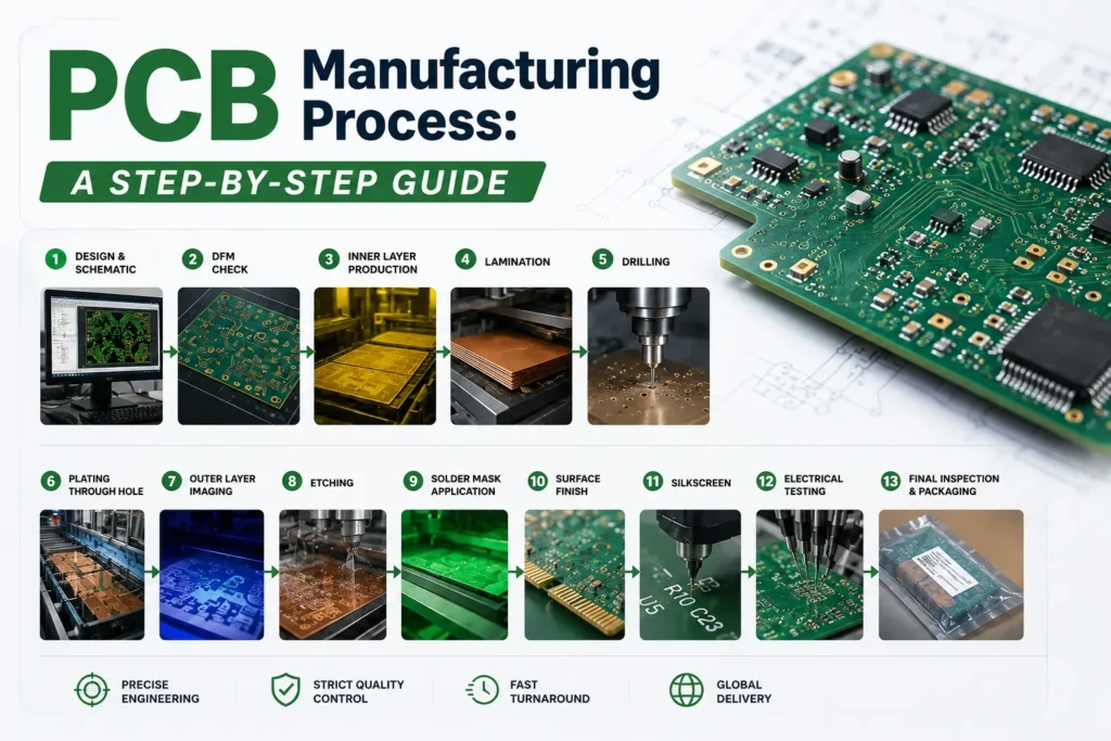
PCB Manufacturing Process: A Step-by-Step Guide
 steve ran
July 6, 2026
steve ran
July 6, 2026
Think Deeper with AI:


Introduction
Beginners often mix up PCB manufacturing and PCB assembly. PCB manufacturing means making the bare board. PCB assembly, also called PCBA, means soldering components onto that board.
This guide focuses mainly on bare PCB manufacturing. You will also see short notes on how each step affects later assembly, cost, and lead time.
Step 1: Gerber File Review and CAM Preparation
PCB manufacturing starts with your production files. Most PCB manufacturers need Gerber files, drill files, a board outline, and basic order specs. For multilayer or controlled impedance boards, they may also need a stack-up drawing and impedance notes.
Gerber files describe copper layers, solder mask, silkscreen, paste layers, and board shape. Drill files show hole sizes and hole locations. The board outline tells the factory where to cut the final board.
After file upload, CAM engineers review the data. CAM means computer-aided manufacturing. The CAM team turns design output into factory-ready production data.
DFM means design for manufacturability. A DFM check finds design choices that may cause defects, delays, or extra cost. For beginners, this step can prevent many common order problems.
Panelization also happens during CAM preparation. A production panel holds many boards together so machines can process them at once. The panel may include tooling holes, rails, coupons, and breakout tabs.
Get a PCB Manufacturing Review
If you have Gerber files ready, send them to HXD Circuit for a practical PCB quote and manufacturability review
Get StartedStep 2: Material Preparation
Most standard PCBs use FR-4. FR-4 is a glass-reinforced epoxy laminate with copper bonded to one or both sides. It gives the board mechanical strength and electrical insulation.
The factory chooses material based on your order specs. Common specs include board thickness, copper weight, layer count, and laminate type.
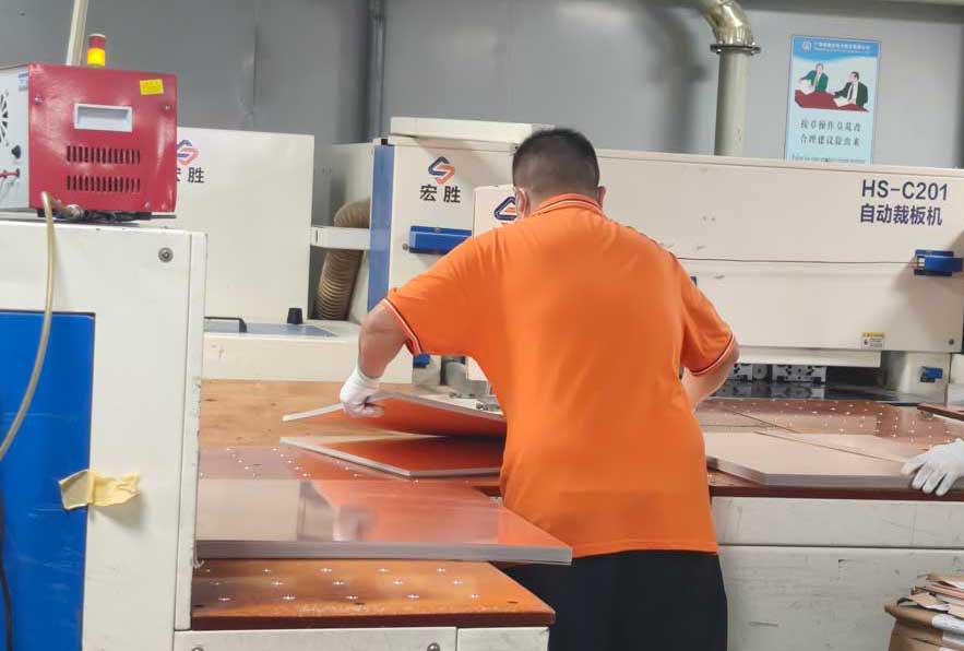
Copper thickness also matters. Many standard boards use 1 oz copper. Higher copper weight can carry more current, but it can raise cost and affect trace spacing rules.
Board thickness affects strength, connector fit, impedance, and mechanical assembly. A common value is 1.6 mm, but thinner and thicker options exist.
Material choice affects cost and performance because different laminates offer different properties. You should avoid unusual materials unless the design needs them.
You can use our Online PCB Material Selector to choose the right material for your project.
Step 3: Inner Layer Imaging and Etching
Multilayer PCBs have copper layers inside the board. These layers may carry signals, power, or ground. The factory forms these inner copper patterns before lamination.
The process uses photoresist. Photoresist is a light-sensitive film that protects selected copper areas.
Etching removes copper that does not belong in the final circuit. The remaining copper becomes traces, pads, and planes.
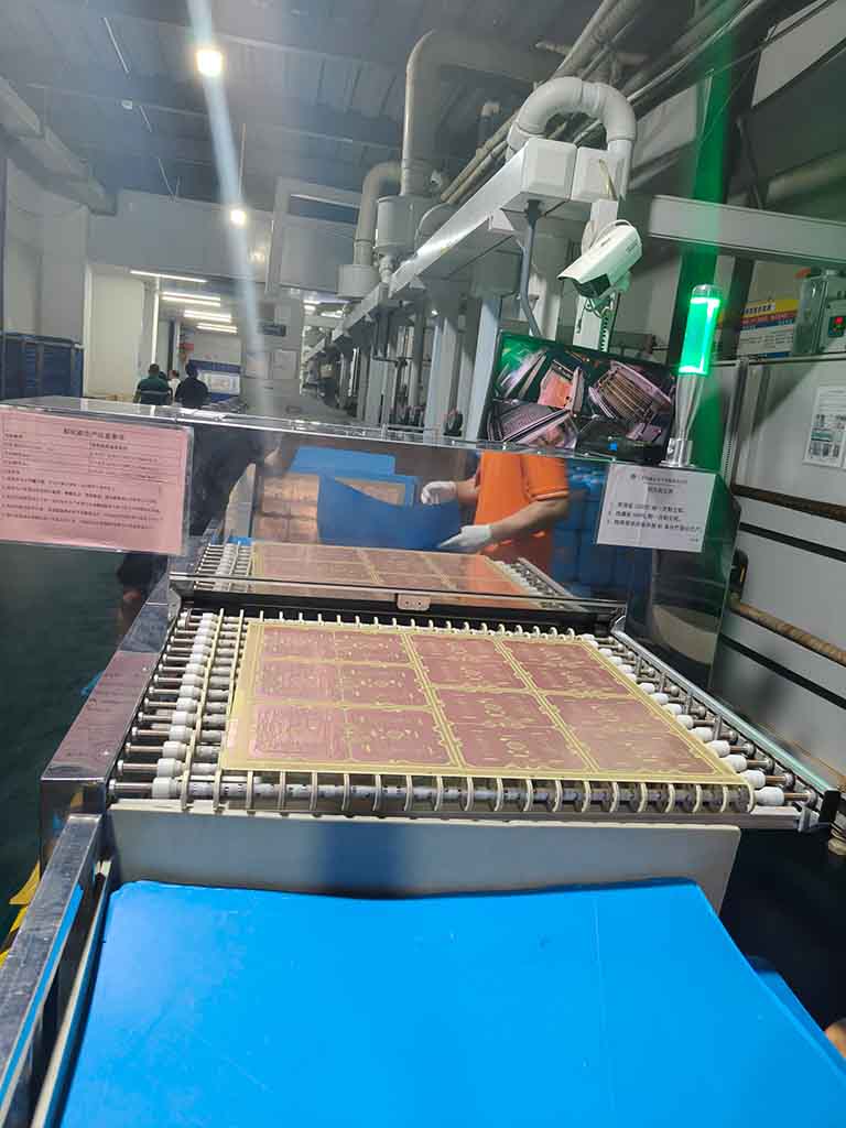
Inner layer inspection matters because defects can become trapped inside the board after lamination. Many factories use AOI, or automated optical inspection, to check inner layers before pressing them together.
Step 4: Layer Lamination for Multilayer PCBs
Lamination bonds PCB layers into one solid board. This step applies mainly to multilayer PCBs. A simple 2-layer board may not need the same multilayer lamination flow.
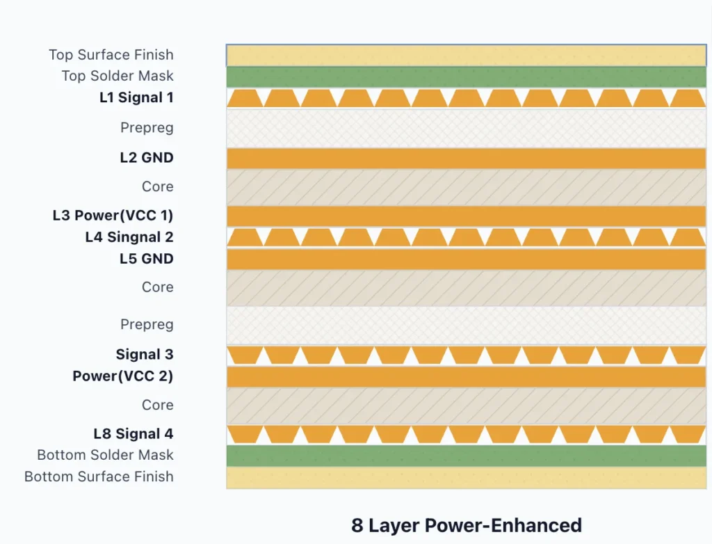
A multilayer stack-up uses cores, prepreg, and copper foil. A core is a cured laminate with copper. Prepreg is a resin-rich fiberglass sheet that bonds layers together during heat and pressure.
During lamination, the factory stacks the layers in the correct order. Alignment pins or optical systems keep the layers in position.
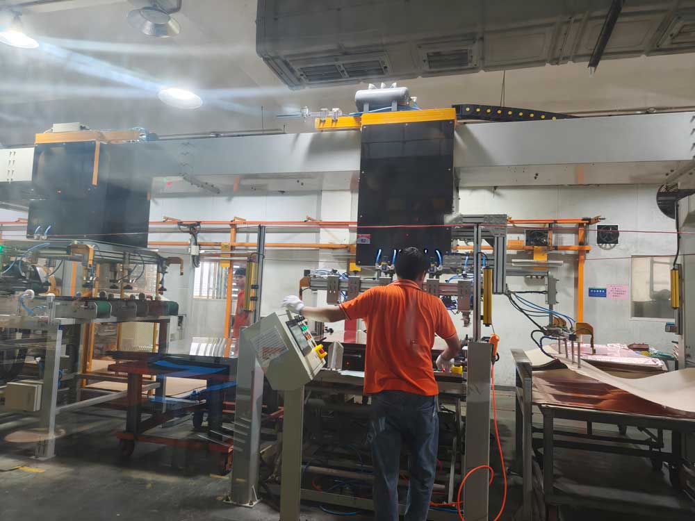
Manufacturers laminate the stack under carefully controlled heat and pressure to form a rigid multilayer PCB.
Layer alignment matters. Poor alignment can shift inner layers away from drilled holes. That can reduce annular ring and create reliability risks.
Step 5: PCB Drilling
Drilling creates holes in the PCB panel. These holes may serve component leads, mounting screws, test points, or vias.
Mechanical drilling uses small drill bits. It works for through holes and many standard vias. The drill passes through the panel and creates holes from top to bottom.
Laser drilling creates smaller holes for HDI boards. HDI means high-density interconnect. These boards may use microvias, blind vias, and fine-pitch components.
Common PCB via types include:
| Hole Type | Meaning | Common Use |
|---|---|---|
| Through hole | Passes through the full board | Component leads, connectors, vias |
| Via | Conductive hole between layers | Signal and power connections |
| Blind via | Connects outer layer to inner layer | HDI designs |
| Buried via | Connects inner layers only | Advanced multilayer boards |
| Non-plated hole | No copper plating inside | Mounting holes or mechanical features |
Drill accuracy affects plating and assembly. If a hole shifts, the drill may cut too much copper from the pad. If a hole is too small, plating may become harder to control. If a component hole is wrong, assembly may fail.
You should check the manufacturer’s minimum drill size before placing small vias.
Step 6: Electroless Copper and Copper Plating
After drilling, the hole walls expose bare laminate. Laminate does not conduct electricity. The factory must coat the hole walls with copper.
The first copper layer often comes from electroless copper. This chemical process deposits a thin copper layer on hole walls without using an electric current. It creates a conductive seed layer.
Then electrolytic copper plating adds more copper. Electric current builds copper thickness on surfaces and inside plated holes.
This step creates plated through holes and conductive vias. A via only works when copper connects the top layer, inner layers, or bottom layer as designed.
Copper thickness control matters. Too little copper can reduce reliability. Too much copper can affect hole size and final dimensions. For designs with higher current, copper thickness also affects heat and voltage drop.
Step 7: Outer Layer Imaging and Etching
After drilling and plating, the factory forms the outer layer copper pattern. This pattern includes final traces, pads, copper pours, and planes.
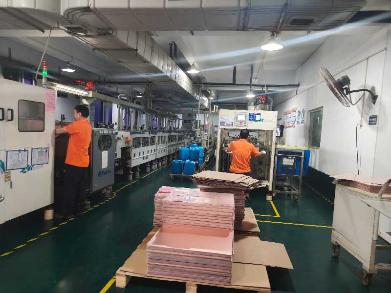
The process is similar to inner layer imaging. The factory applies photoresist and exposes the circuit pattern. It then develops it, plates copper where needed, and etches away unwanted copper.
Trace width and spacing become important here. Thin traces and narrow gaps need tighter process control. If the design pushes beyond the factory’s standard limits, cost and risk can rise.
Your should understand three common copper defects:
| Defect | Possible Cause |
|---|---|
| Open | Over-etching, scratch, or poor imaging |
| Short | Under-etching, contamination, or spacing too tight |
| Over-etching | Process control issue or features too fine |
Good design rules lower these risks. Use trace width, spacing, and annular ring values that match the factory’s stated capability.
Step 8: Solder Mask Application
Solder mask is the colored protective coating on a PCB. Green is common, but many manufacturers also offer black, blue, red, white, yellow, and other colors.
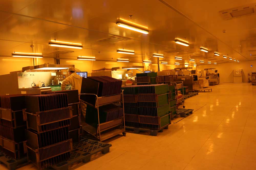
Solder mask covers most copper areas. It leaves pads exposed so components can solder to them later.
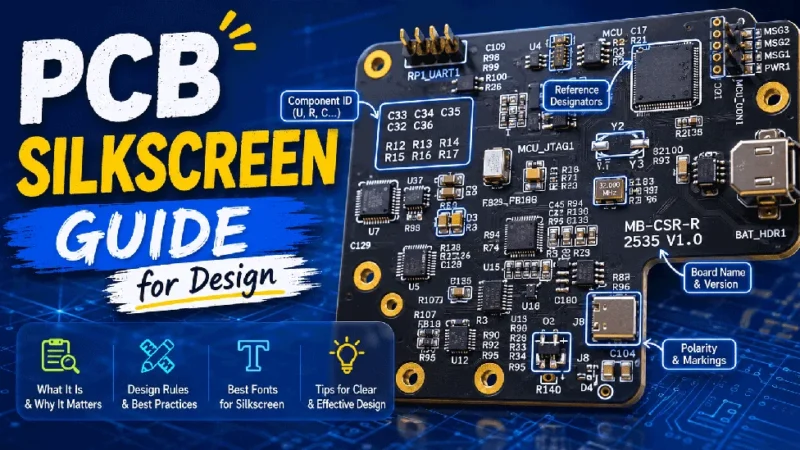
Step 9: Silkscreen Printing
Silkscreen adds readable markings to the PCB. These markings can include reference designators, polarity marks, pin 1 marks, logos, revision numbers, date codes, and assembly notes.
Clear silkscreen helps assembly and repair. A technician can identify parts faster. An engineer can debug the board more easily.
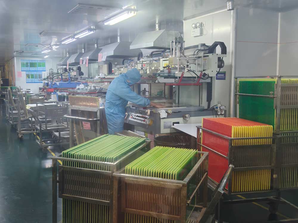
Silkscreen does not carry current, but it still affects usability. Beginners should treat it as part of the product documentation.
Step 10: Surface Finish
Copper pads oxidize when exposed to air. A surface finish protects exposed copper and prepares pads for soldering.
Different surface finishes fit different design needs.
| Surface Finish | Best For | Advantages | Limits |
|---|---|---|---|
| HASL | Simple prototypes and larger pads | Low cost, familiar process | Less flat than other finishes |
| Lead-free HASL | RoHS-friendly general boards | Low cost, lead-free option | Not ideal for fine-pitch parts |
| ENIG | Fine-pitch parts, BGAs, longer shelf life | Flat surface, good solderability | Higher cost than HASL or OSP |
| OSP | Cost-sensitive boards with quick assembly | Flat, simple, lead-free | Shorter shelf life, handling sensitive |
| Immersion silver | High-speed or solderability-sensitive designs | Flat, good electrical performance | Can tarnish if stored poorly |
| Immersion tin | Press-fit and flat-pad needs | Flat and lead-free | Can have storage and whisker concerns |
For many projects, ENIG offers a safe and flat finish, especially for small pads. HASL can work for simple boards with larger parts. OSP can reduce cost when boards move quickly into assembly.
Step 11: Profiling, Routing, V-Cut, and Panelization
After the board surface is complete, the factory shapes the panel into final boards or assembly panels.
Routing uses a cutting tool to create the board outline, slots, and cutouts. It works well for complex shapes and internal openings.
V-cut, also called V-scoring, cuts shallow grooves between rectangular boards. Assemblers can separate boards after component assembly. V-cut works best for straight-line separations.
Panelization matters for assembly. SMT machines need stable panels, fiducials, and enough rail area. Poor panel design can cause handling problems, placement errors, or board damage.
Step 12: Electrical Testing and Final Inspection
Electrical testing checks whether the board has open circuits or short circuits. An open means a copper path does not connect. A short means two areas connect when they should stay separate.
Factories often use flying probe testing for prototypes and small batches. A flying probe tester uses moving probes to touch test points and check net connections. For larger batches, a fixture test may reduce test time.
Testing reduces assembly risk. If a bare board has a short or open, assembly wastes components, labor, and time. Bare-board testing catches many problems before technicians solder parts onto the board.
What Files and Specs Do You Need Before PCB Manufacturing?
A manufacturer can quote and build faster when you send complete data. Missing specs often cause engineering questions and delays.
Prepare these items before ordering:
| Item | Why It Matters |
|---|---|
| Gerber files | Define copper, solder mask, silkscreen, paste, and outline layers |
| Drill files | Define plated and non-plated holes |
| Board outline | Shows final board shape and cutouts |
| Layer count | Sets stack-up and process route |
| Material | Affects cost, heat, signal performance, and strength |
| Board thickness | Affects fit, stiffness, and impedance |
| Copper weight | Affects current capacity and manufacturing limits |
| Surface finish | Affects solderability, shelf life, and cost |
| Solder mask color | Affects appearance and sometimes inspection contrast |
| Silkscreen color | Affects readability |
| Quantity | Affects unit cost and production method |
| Testing needs | Defines electrical test, impedance test, or special inspection |
| Controlled impedance notes | Needed for high-speed designs |
| Special requirements | Slots, countersinks, edge plating, carbon ink, peelable mask, or via filling |
Request a free PCB quote today and let our team help turn your design into production-ready circuit boards.
A clear order note can prevent confusion. Include board thickness, copper weight, finish, mask color, and quantity in the same quote request.
Conclusion
The PCB manufacturing process starts with design files and ends with a tested bare circuit board.
You do not need to master every factory detail before ordering. You do need clean files, clear specs, and a basic understanding of how design choices affect cost, lead time, and quality.
FAQ